2026 Top Tips for PCB Layout Design Techniques and Best Practices?
In today's fast-paced electronics world, effective PCB layout is crucial. A well-designed printed circuit board not only optimizes performance but also enhances reliability. Designing a PCB involves numerous techniques and best practices that can significantly impact the final product. Understanding these practices is essential for engineers and hobbyists alike.
Every layout tells a story. A flawed PCB layout can lead to signal interference and reduced functionality. Small details matter, like trace width and spacing. Choosing the right materials makes a difference. However, many designers overlook these aspects, leading to costly errors. Balancing aesthetics with functionality is challenging.
Effective communication between team members also plays a vital role. Collaboration can lead to innovative solutions and better designs. Yet, this aspect is frequently neglected. Engineering is an iterative process, and reflecting on past designs can foster improvement. Acknowledging mistakes creates a pathway to better decisions in future PCB layout endeavors.

Essential Principles of PCB Layout Design for Beginners
When starting with PCB layout design, it’s crucial to grasp essential principles. Understanding the basics will help prevent common pitfalls. For example, maintaining a clear ground plane reduces noise. It also ensures better signal integrity. Beginners often overlook this aspect, leading to interference issues.
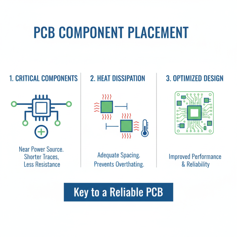
The placement of components is another key factor. A well-organized layout streamlines routing. However, it’s easy to overcrowd a board. Doing so can create complicated paths for traces. This complexity may introduce errors. Instead, aim for a balance. Keep some space around components to ease troubleshooting and modifications.
Additionally, following design rules is vital. It’s tempting to ignore them for a quick design. This can lead to significant problems down the line. Set design constraints early on. Regularly check your work against these standards. Reflect on your design choices. Ask for feedback from peers. This practice improves your layout over time.
Best Practices for Minimizing Electromagnetic Interference (EMI)
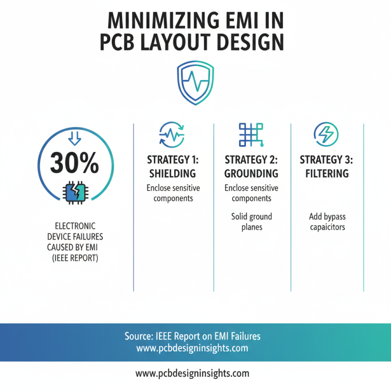
Minimizing electromagnetic interference (EMI) is crucial in PCB layout design. According to a report from the IEEE, EMI causes up to 30% of failures in electronic devices. This highlights the need for effective strategies to mitigate interference.
One key technique is grounding. A good ground plane can significantly reduce EMI. It helps maintain consistent voltage levels and minimizes return path loops. However, many designers overlook proper grounding techniques, leading to performance issues.
Another effective method is component placement. Positioning sensitive components away from noisy ones is essential. Keep high-frequency components isolated. This simple practice can be a game changer. A study by IPC indicated that 50% of devices could avoid EMI issues if proper placement principles were followed.
In addition, routing techniques are vital. Minimizing trace lengths reduces inductance. However, many times, designers ignore this detail, which can lead to unwanted coupling. Good layout practices can improve signal integrity and reduce EMI. These practices are simple yet often ignored, leading to costly redesigns.
Importance of Grounding and Power Distribution in PCB Design
Grounding and power distribution in PCB design should never be overlooked. These aspects directly affect a circuit board's performance and reliability. Proper grounding minimizes noise and ensures stable operation. It creates a reference point for all signals. A poor grounding scheme can lead to erratic behavior in sensitive components.
Power distribution requires careful planning. It’s essential to consider the paths that power takes throughout the PCB. Wider traces can help reduce voltage drops and heat generation. However, making traces too wide can lead to wasted space. Striking a balance here can be challenging. Use ground planes effectively; they provide low-resistance paths and reduce electromagnetic interference.
Inadequate grounding often leads to issues that are hard to diagnose. Designers must regularly review their grounding strategies. Mistakes can surface as intermittent failures or disrupted signals. Always question whether the grounding scheme is truly robust and if every component is receiving stable power. Reflecting on these strategies can lead to improvements in future designs.
Utilizing Design Software Tools for Enhanced PCB Layout Efficiency
Effective PCB layout is crucial in today’s electronic design landscape. Utilizing advanced design software tools can significantly enhance layout efficiency. Software aids in optimizing component placement and routing. According to a report by the IPC, nearly 70% of PCB design time is spent on layout adjustments. This highlights the importance of using tools that streamline the design process.
Many designers overlook the benefits of simulation tools. These programs can detect potential issues early, reducing costly revisions. Research indicates that early detection of design flaws can save up to 30% on project costs. Yet, many professionals still rely on manual checks, leading to inefficiencies and errors. Investing in simulation can lead to a more robust design strategy.
Design parameters vary widely across industries. However, data suggests that 75% of beginners struggle with layout complexities. They often ignore best practices, impacting overall performance. Regular training on software features can remedy this. It creates a knowledgeable workforce capable of navigating intricate designs. Encouraging continuous learning is essential, yet it remains a challenge for many organizations.
2026 PCB Layout Design Techniques and Best Practices
This chart illustrates the effectiveness of various PCB layout design techniques based on an efficiency score derived from extensive industry surveys. The techniques include using design software tools, following best practices in component placement, and ensuring proper signal integrity.