2026 Best PCB Layout Design Tips for Optimal Performance
In the evolving world of electronics, PCB layout plays a crucial role in device performance. Expert John Murphy, recognized for his innovative designs, emphasizes, "A well-structured PCB layout can make or break a project." His wisdom highlights the importance of careful planning and execution in this field.
When designing PCB layouts, attention to detail is non-negotiable. Every trace and component placement matters. Common pitfalls exist, such as inadequate spacing, which can lead to signal interference. Many designers overlook thermal management. Proper heat dissipation is vital for longevity.
Every designer faces challenges. Even seasoned professionals encounter issues in layout design. Reflecting on past mistakes can be enlightening. Continuous improvement is part of the journey in mastering PCB layout. Balancing creativity and technical specifications requires ongoing effort and learning. The pursuit of optimal performance is ongoing and requires dedication.

Understanding PCB Layout Basics for Optimal Performance
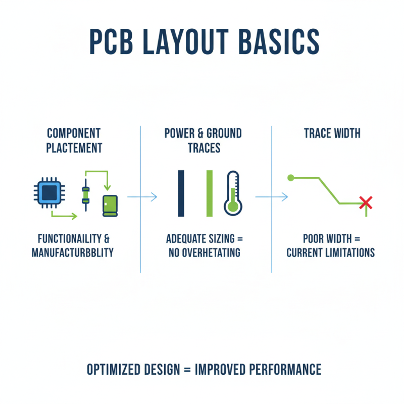
Understanding the basics of PCB layout design is essential for improved performance. The placement of components should aid in both functionality and manufacturability. Power and ground traces must be adequately sized to reduce the risk of overheating. Poor trace width can lead to current limitations, affecting the entire board. Designers often overlook this critical aspect.
Signal integrity is another vital element to consider. Traces should be kept as short and direct as possible. Longer traces usually introduce noise and signal loss. Using controlled impedance traces helps maintain signal quality, but this can be neglected by many. The layer stack-up also impacts performance; misalignment can cause various issues.
Grounding is often underestimated. A well-designed ground plane minimizes interference but many layouts fail at this stage. Additionally, consider component orientation; it can influence heat dissipation and routing efficiency. Mistakes in these areas often arise from a lack of foresight. Reflecting on these details can lead to better PCB designs and overall performance.
Importance of Layer Stackup in PCB Design
Layer stackup significantly impacts PCB performance. It's not just a design choice; it's a foundation. A well-planned stackup reduces electromagnetic interference (EMI). According to research, nearly 75% of PCB failures relate back to improper layout decisions, including layer arrangement.
The choice of materials and their arrangement affects thermal performance. Up to 40% of PCB users have reported thermal management issues that could have been addressed through better stackup practices. For instance, using dielectric materials with specific thickness can enhance signal integrity and minimize crosstalk. The ideal thickness often ranges from 5 to 50 mils, depending on the application.
However, many designers overlook this critical aspect. They might prioritize component placement over layer configuration, leading to inefficiencies. It's essential to reflect on your design choices to ensure optimal performance. Engaging in a thoughtful review of your layer stackup can reveal glaring inefficiencies and unlock the full potential of your PCB design.
2026 PCB Layer Stackup Impact on Performance
This chart illustrates the impact of different PCB layer stackups on signal integrity, measured in decibels (dB). As the number of layers increases, the signal integrity improves, demonstrating the importance of proper layer stackup in PCB design for optimal performance.
Best Practices for Component Placement and Routing
When designing a PCB, component placement is crucial. A clean layout minimizes interference.
Studies show that poorly placed components can increase electromagnetic interference (EMI) by up to 30%.
Keeping sensitive components away from noisy ones is essential. For example, place analog devices far from high-speed digital ones. This simple move can enhance signal integrity.
Routing is another key factor. Shorter traces reduce resistance and inductance.
A report cited that 25% of devices failed due to inefficient routing practices.
Keep traces as short as possible, especially for high-frequency signals. Routing them close to the reference ground can also help.
However, it's easy to neglect via placement, leading to increased signal loss.
Think about heat distribution too. Components that generate heat should be spaced appropriately. This prevents nearby parts from overheating.
A study found that improper thermal management can shorten a device’s lifespan by 40%.
It’s easy to overlook this detail, but doing so can lead to costly failures. Reflect on the layout choices.
Small adjustments can make a significant impact on performance.
Effective Grounding Techniques for Enhanced Signal Integrity
Grounding techniques are crucial for signal integrity in PCB design. Poor grounding can introduce noise and distort signals. This leads to erratic performance in circuits.
Solid grounding reduces these risks significantly. It's vital to place ground plane layers wisely. Have them close to the signal traces.
One key tip is to use a star ground configuration. This minimizes ground loops. Loops can create unwanted interference.
Another effective approach is to separate analog and digital grounds. This isolation helps maintain clean signals. Be cautious, however, as poorly implemented separation may cause more issues.
Pay attention to the via placements. Using too many vias can increase inductance. This can negatively impact the signal. Keep your ground connections short and direct.
Strive for a clean layout, but imperfections happen. Regularly revisit your designs for potential flaws.