In the rapidly evolving electronics industry, the significance of selecting the appropriate PCB manufacturing and assembly process cannot be overstated. According to a market report by Research and Markets, the global printed circuit board (PCB) market is projected to reach USD 85.09 billion by 2027, with a compound annual growth rate (CAGR) of 3.8% from 2020. Such growth underscores the critical role of effective PCB production methodologies in ensuring quality, reliability, and cost-effectiveness in electronic devices.
Choosing the right PCB manufacturing and assembly process involves a comprehensive understanding of various options available in the market. Factors such as complexity, volume, turnaround time, and cost all play a pivotal role in this decision-making process. A report by IPC, the Association Connecting Electronics Industries, highlights that the efficiency of the PCB assembly process directly impacts the overall production timeline, emphasizing the need for manufacturers to align their processes with project requirements to avoid delays and exceed customer expectations.
By making informed choices in PCB manufacturing and assembly, businesses can not only enhance their product functionality but also maintain a competitive edge in a crowded marketplace. As they navigate through the complexities of various techniques and technologies, understanding industry standards and leveraging available resources will be essential for successful project outcomes.
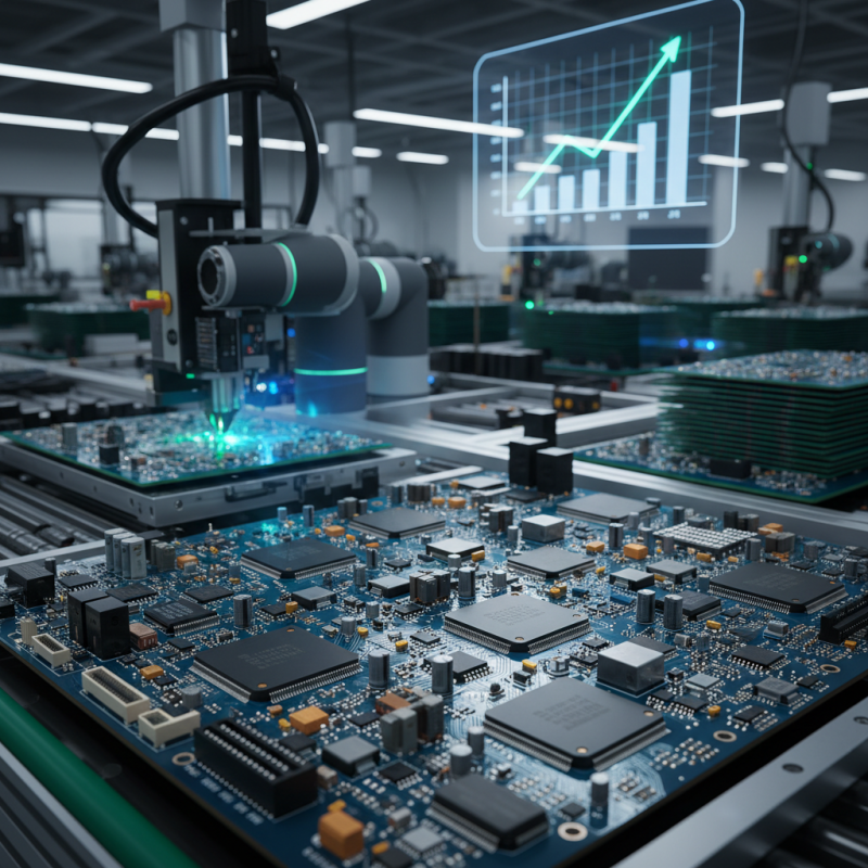
Understanding the basics of PCB manufacturing is crucial for anyone looking to design and produce functional electronic assemblies. The process begins with the creation of a schematic, which serves as a blueprint for the circuit board. This schematic guides the layout of components, traces, and vias on the PCB. Using specialized software, designers can simulate and optimize circuits, ensuring that the final layout adheres to the necessary electrical and mechanical specifications.
Once the design is finalized, the actual manufacturing process takes place, involving several key steps. The creation of the PCB starts with material selection, typically involving a copper-clad laminate base. After applying the desired pattern using photolithography, the copper is etched away to leave the required circuitry. Following this, additional processes such as drilling, plating, and surface finishing are executed to enhance conductivity and protect the board.
Finally, quality control measures, including visual inspections and testing, are essential to ensure that the PCB meets the
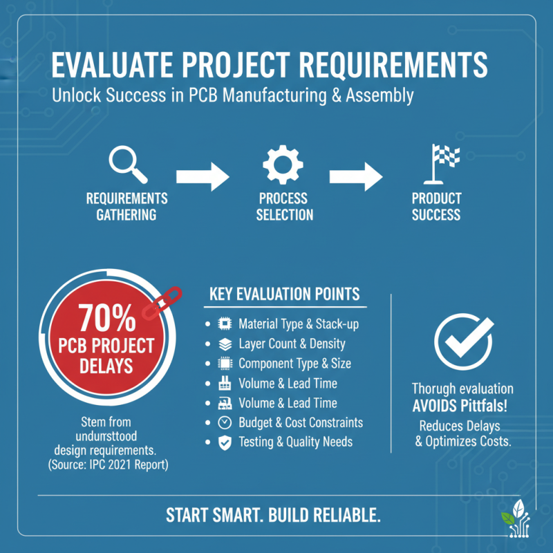
Evaluating project requirements is a crucial first step in selecting the appropriate PCB manufacturing and assembly process. Understanding the specific needs of your project can dramatically influence the decision-making process and ultimately determine the success of your product. According to the IPC's 2021 report, it is estimated that around 70% of PCB project delays stem from misunderstandings of design requirements. Therefore, conducting a thorough evaluation at the outset helps to avoid common pitfalls that can arise from vague specifications or improper assessments.
Key factors to consider include the board's complexity, the expected volume of production, and application-specific requirements such as environmental conditions or regulatory compliance. For instance, projects requiring high-density interconnect (HDI) boards will need advanced manufacturing techniques like laser drilling and microvias, which significantly differ from those used in simpler designs. Additionally, the 2022 Global Electronics Manufacturing Services (EMS) report highlights that customizing assembly techniques to fit unique design specifications can lead to a 30% increase in efficiency during production, underlining the importance of aligning your assembly process with your project's technical demands.
By carefully assessing these factors, including cost constraints and timelines, you can better match your project's PCB manufacturing and assembly needs, thus facilitating smoother development cycles and achieving desired outcomes more efficiently.
Selecting the right manufacturing process for printed circuit boards (PCBs) is crucial for the success of any electronic project. The choice significantly impacts not just the quality and reliability of the final product, but also costs and production timelines. According to a report by IPC, approximately 90% of design defects stem from the manufacturing process, underscoring the importance of integrating manufacturing considerations early in the design stage. Factors such as the complexity of the circuit design, volume of production, and the materials involved must be seriously evaluated.
Different manufacturing processes such as surface mount technology (SMT) and through-hole technology present distinct advantages and challenges. SMT, which has been shown to reduce the footprint of circuits by up to 50%, is ideal for high-density designs and offers faster assembly speeds. In contrast, through-hole technology might be preferable for components that require greater durability.
The electronics manufacturing services (EMS) market is projected to reach $525.16 billion by 2027, which reflects the growing need for optimized processes to meet consumer demands for both speed and precision. Thus, understanding these dynamics is essential for selecting the manufacturing method that aligns with project requirements and market trends.
When evaluating assembly techniques for your PCB project, it is essential to understand the various methods available and their implications on production efficiency and cost. Traditional through-hole assembly, while reliable, tends to be more labor-intensive and time-consuming compared to surface mount technology (SMT). According to industry reports, SMT accounts for approximately 85% of today's PCB assembly, largely due to its ability to accommodate higher component densities and reduced manufacturing times. This shift not only enhances the compactness of devices but also supports more automated assembly processes, reducing overall labor costs.
Furthermore, each assembly technique presents unique challenges and benefits that can significantly impact your project. For instance, the choice between manual and automated processes can affect lead times and scalability. A report from IPC indicates that fully automated lines can yield up to 30% higher productivity compared to manual assembly. However, this higher output comes with the need for substantial upfront investment in equipment and training. Additionally, depending on the complexity of your PCB design and the materials used, specific techniques such as reflow soldering or wave soldering may be more suited to your needs. Understanding these factors is crucial for making informed decisions that align with your project goals and budget constraints.
| Assembly Technique | Advantages | Disadvantages | Best Use Case |
|---|---|---|---|
| Surface Mount Technology (SMT) | High component density, automated process | Requires precise manufacturing, less suitable for larger components | Compact PCBs, high-volume production |
| Through-Hole Technology (THT) | Strong mechanical bonds, easier for prototyping | More space-consuming, slower assembly process | High reliability needs, large components |
| Mixed Technology | Combines benefits of both SMT and THT | Complex assembly process, higher cost | Varied component types, custom PCBs |
| Chip-on-Board (COB) | Compact size, reduced assembly costs | Sensitive to environmental factors, requires careful handling | Highly miniaturized devices, specific applications |
When selecting a PCB manufacturing and assembly process, cost considerations play a crucial role in the overall success of your project. According to a recent study by IPC, the average cost for PCB fabrication can range from $1 to $10 per square inch, depending on factors such as complexity, materials used, and volume of production. For instance, low-volume projects often incur higher costs per unit due to setup and tooling expenses. As such, it's essential to weigh the cost-effectiveness of both low-volume and high-volume production options, finding a balance that meets the project's financial constraints without compromising on quality.
Tips: To reduce PCB production costs, consider opting for standard materials and simpler designs where possible. Utilizing a design for manufacturability (DFM) approach can help identify potential cost savings early in the design phase, preparing your project for a more efficient manufacturing process.
Additionally, the choice between surface mount technology (SMT) and through-hole technology (THT) can significantly impact your budget. SMT is generally favored for higher density and smaller size PCBs, leading to reduced assembly costs. According to the 2022 IPC Market Research Report, companies that adopted SMT reduced their assembly costs by approximately 25% compared to those that primarily used THT. Therefore, choosing the right technology upfront can provide substantial savings in both material and labor costs.
: The first step in the PCB manufacturing process is the creation of a schematic, which serves as a blueprint for the circuit board, guiding the layout of components, traces, and vias.
Designers can use specialized software to simulate and optimize circuits, ensuring that the final layout adheres to necessary electrical and mechanical specifications before manufacturing.
The manufacturing process typically starts with a copper-clad laminate base, which serves as the foundational material for the PCB.
Key processes include photolithography to apply patterns, etching to remove excess copper, drilling, plating, and surface finishing to enhance conductivity and protect the board.
Quality control measures, such as visual inspections and testing, are essential to ensure that the PCB meets project requirements before moving on to assembly.
Factors influencing PCB fabrication costs include complexity, materials used, volume of production, and setup and tooling expenses, particularly for low-volume projects.
To reduce production costs, consider using standard materials, simpler designs, and adopting a design for manufacturability (DFM) approach to identify cost-saving opportunities early in the design phase.
SMT is generally preferred for higher density and smaller size PCBs as it can lead to reduced assembly costs, with companies adopting SMT experiencing approximately 25% lower assembly costs compared to those using THT primarily.
| Cookie | Duration | Description |
|---|---|---|
| cookielawinfo-checkbox-analytics | 11 months | This cookie is set by GDPR Cookie Consent plugin. The cookie is used to store the user consent for the cookies in the category "Analytics". |
| cookielawinfo-checkbox-functional | 11 months | The cookie is set by GDPR cookie consent to record the user consent for the cookies in the category "Functional". |
| cookielawinfo-checkbox-necessary | 11 months | This cookie is set by GDPR Cookie Consent plugin. The cookies is used to store the user consent for the cookies in the category "Necessary". |
| cookielawinfo-checkbox-others | 11 months | This cookie is set by GDPR Cookie Consent plugin. The cookie is used to store the user consent for the cookies in the category "Other. |
| cookielawinfo-checkbox-performance | 11 months | This cookie is set by GDPR Cookie Consent plugin. The cookie is used to store the user consent for the cookies in the category "Performance". |
| viewed_cookie_policy | 11 months | The cookie is set by the GDPR Cookie Consent plugin and is used to store whether or not user has consented to the use of cookies. It does not store any personal data. |