How to Design Advanced PCB for High Performance and Reliability
In the rapidly evolving landscape of electronics, designing advanced PCBs (Printed Circuit Boards) has become essential for achieving high performance and reliability in various applications, from consumer electronics to industrial machinery. Dr. Emily Chen, a leading expert in the field of PCB design, emphasizes the significance of this evolution: "The future of electronic devices hinges on our ability to innovate with advanced PCB technologies, ensuring they meet the demands of both functionality and durability."
With advancements in materials, design methodologies, and manufacturing techniques, engineers are now tasked with creating PCBs that not only perform well under demanding conditions but also withstand the test of time. High-frequency signals, thermal management, and signal integrity are just a few of the challenges that require a sophisticated approach in PCB design. Understanding these complexities is crucial in developing solutions that enhance product longevity and maximize performance.
As the market continues to push the boundaries of what is possible, the focus on advanced PCB design is more relevant than ever. This article aims to explore key strategies and best practices for engineers and designers to elevate their PCB designs, ensuring they can keep pace with the technological advancements that define today's electronic landscape.
Understanding PCB Basics: Key Concepts for High Performance Design
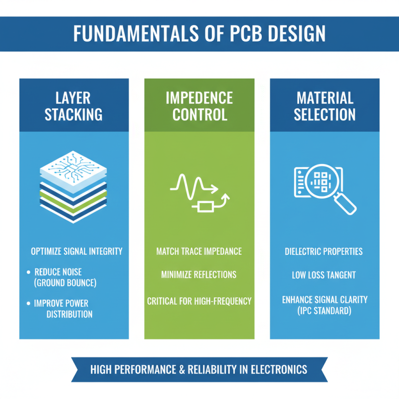
Understanding the fundamentals of PCB design is crucial for achieving high performance and reliability in electronic applications. Key concepts such as layer stacking, impedance control, and material selection play a significant role in the overall design strategy. For instance, according to the IPC's "PCB Design Standard," utilizing the right dielectric materials can significantly affect signal integrity by minimizing loss and distortion, which is critical in high-frequency applications. It's reported that optimizing layer count and ensuring proper power distribution can decrease the likelihood of ground bounce, a common issue that can lead to signal degradation.
Furthermore, thermal management is a vital aspect often overlooked in the early design stages. Data from the "2019 PCB Thermal Management Report" indicates that poor heat dissipation can reduce the reliability of components by up to 50%. Implementing thermal vias and utilizing copper planes effectively can aid in maintaining optimal operating temperatures, thereby enhancing performance and longevity. As PCBs are integral in various sectors including automotive, aerospace, and consumer electronics, understanding these basics will empower designers to craft advanced PCBs that not only meet performance specifications but also uphold reliability under demanding conditions.
Materials Selection: Choosing the Right Components for Reliability
In the realm of PCB design, the selection of materials plays a pivotal role in influencing the performance and reliability of electronic devices. Industry reports suggest that approximately 75% of PCB failures can be traced back to material selection mistakes. As technology advances, the demand for high-performance PCBs has increased, necessitating a comprehensive understanding of the properties of various materials. For instance, materials like FR-4 remain popular due to their excellent balance of cost, performance, and thermal properties, while high-frequency applications often call for materials like PTFE or ceramic to ensure signal integrity.
Reliability in PCBs is fundamentally linked to their ability to withstand environmental stresses, including temperature fluctuations, humidity, and mechanical vibrations. According to a 2022 IPC report, using high-temperature laminates can enhance durability. These materials typically demonstrate greater resistance to thermal degradation, ensuring that PCBs maintain functionality in extreme conditions. Furthermore, the consideration of dielectric strength and thermal conductivity is critical when selecting components, as these factors directly impact signal performance and longevity. Therefore, choosing the right materials is not just a design choice; it is a crucial factor that dictates the overall reliability and effectiveness of high-performance PCBs in diverse applications.
How to Design Advanced PCB for High Performance and Reliability - Materials Selection: Choosing the Right Components for Reliability
| Component Type |
Material |
Thermal Conductivity (W/mK) |
Dielectric Constant |
Operating Temperature (°C) |
Reliability Rating |
| Capacitor |
Ceramic |
30 |
5.0 |
-55 to 125 |
A |
| Resistor |
Metal Film |
15 |
3.0 |
-55 to 155 |
A+ |
| Inductor |
Ferrite |
5 |
4.5 |
-40 to 150 |
B |
| Connector |
Plastic (Polycarbonate) |
N/A |
2.5 |
-40 to 120 |
A |
| PCB Base Material |
FR-4 |
0.5 |
4.0 |
-40 to 130 |
A |
Layer Stack-Up Design: Optimizing PCB Layout for Signal Integrity
When designing advanced printed circuit boards (PCBs) for high performance and reliability, the layer stack-up is a critical factor that significantly impacts signal integrity. A well-optimized layer stack not only improves electrical performance but also minimizes issues such as crosstalk and EMI (Electromagnetic Interference). According to a report by IPC, as many as 60% of PCB failures can be traced back to design issues related to the layer stack configuration, underscoring the importance of this aspect in the development process.
In practical terms, managing the dielectric thickness and material selection between layers can be crucial. For instance, using advanced materials like low-loss dielectrics can enhance signal integrity at high frequencies, which is essential for applications in telecommunications and high-speed data transfer. Moreover, a balanced approach to the arrangement—ensuring a proper distribution of power and ground planes—can help achieve a controlled impedance, reducing signal degradation. Research indicates that designs with an optimal layer stack can achieve a 30% reduction in signal loss compared to those with less attention to layer specification.
Furthermore, simulation tools that model electromagnetic behavior in layered structures can provide invaluable insights during the design phase. By utilizing these tools, engineers can predict how changes in layer configuration will affect signal paths, ultimately leading to more robust designs. The incorporation of such simulations has been shown to decrease the time-to-market for new designs by approximately 25%, allowing quicker iterations and refinement in high-performance applications.
Thermal Management Strategies for Advanced PCB Performance
Thermal management is a critical factor in the design of advanced PCBs, directly impacting both performance and reliability. Research from IPC indicates that thermal failure accounts for approximately 40% of all PCB-related issues, making effective thermal management strategies essential. As electronic components become more powerful and compact, generating higher operating temperatures, designers must implement methods that can dissipate heat efficiently to prevent thermal-related failures. Techniques such as implementing thermal vias, using heat sinks, and optimizing copper traces are fundamental in enhancing heat dissipation, thereby increasing the overall reliability of the PCB.
The advancement of materials also plays a significant role in thermal management. High thermal conductivity substrates, like polyimide or ceramic-based materials, are gaining popularity as they offer improved thermal performance. A study by the Electronics Cooling magazine shows that using advanced thermal interface materials (TIMs) can reduce thermal resistance by over 50% compared to conventional options. Moreover, employing thermal simulation tools during the design phase allows engineers to predict temperature distributions within the PCB, enabling proactive adjustments to layout and component placement. By utilizing these innovative thermal management strategies, designers can create robust PCBs capable of enduring high-performance applications while maintaining long-term reliability.
Thermal Management Strategies in PCB Design
Testing and Quality Assurance: Ensuring Reliability in PCB Manufacturing
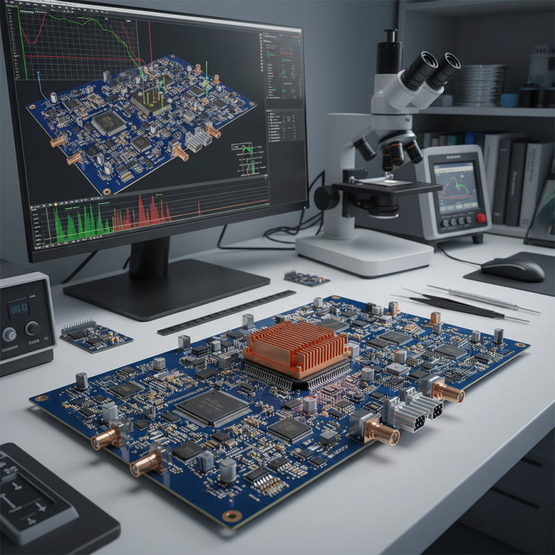
Testing and quality assurance are critical components in ensuring the reliability of printed circuit board (PCB) manufacturing, especially when designing advanced PCBs for high performance. A comprehensive testing strategy should include various methodologies, such as functional tests, thermal profiling, and electrical integrity checks, to identify potential failures before the product reaches the market. Each of these testing phases allows designers to detect weaknesses in the PCB, ensuring that it can withstand both operational stresses and environmental challenges.
Tip: Implementing automated test equipment (ATE) can significantly enhance the efficiency and accuracy of your testing processes. ATE provides consistent results that help pinpoint issues quickly, reducing time-to-market for your designs.
In addition to rigorous testing, maintaining high standards of quality assurance throughout the manufacturing process is essential. This involves not just verifying the final product but also monitoring each step of the PCB assembly, from component sourcing to soldering techniques. Adopting a continuous improvement approach can lead to significant advancements in quality and reliability.
Tip: Regularly conduct process audits and review supplier quality metrics to ensure all materials used meet the highest standards, minimizing the risk of defects in the final PCB.