How to Design a Printed Circuit Board for Your Electronics Project?
Designing a printed circuit board can seem daunting. Many new engineers face challenges with complexity. Yet, creating an effective PCB can lead to successful electronics projects.
A printed circuit board, or PCB, connects electrical components efficiently. Each design starts with a clear purpose. You should plan your layout carefully. Mistakes are common, and it’s easy to overlook connections or component placements. Checking your work is crucial. Use software tools to visualize your design and find potential errors.
Moreover, choosing materials can greatly impact your project. Thicker copper for power applications or specialized substrates for RF circuits might be necessary. Each decision shapes the functionality and reliability of your PCB. Taking the time to reflect on your design choices will enhance your project’s chances of success.
Understanding the Basics of Printed Circuit Board Design
Designing a Printed Circuit Board (PCB) is essential for any electronics project. Understanding the basics is the first step. A well-designed PCB integrates various electronic components on a single board. According to industry reports, the global PCB market reached $62.4 billion in 2022, revealing a growing demand for efficient design practices.
The layout of a PCB can affect performance significantly. Poor signal integrity can lead to malfunctions. Using the right trace widths and spacing is critical. For example, a trace that is too narrow may overheat, while excessive space can cause cross-talk. A report from IPC indicates that 70% of PCB failures arise from design errors. This highlights the need for careful planning and simulation during the design phase.
Prototyping is a vital step. Many designers overlook this phase, rushing to production. This can lead to costly errors. Investing in a prototype can save time and resources later. Feedback from the prototype can guide necessary adjustments. Designers must embrace this iterative process. Reflection on past projects can also yield insights into improving future designs.
Selecting the Right Tools and Software for PCB Design
When designing a printed circuit board (PCB), choosing the right tools is crucial. Begin by considering your project’s complexity. Simple projects may only need basic software. More complex designs benefit from advanced features. Look for tools that offer intuitive interfaces. A user-friendly design streamlines your workflow.
Tips: Familiarize yourself with different software options. Free versions can be limiting but useful for beginners. Consider investing in a robust tool as your skills progress.
Another essential aspect is compatibility. Ensure that the software you choose supports various file types. This can save time when collaborating with others. Also, check the online community around the tools. A strong user community can be a great resource.
Tips: Look for tutorials and forums that can enhance your learning. Discussing with others helps when troubleshooting issues. Don't skip practicing with smaller designs before diving into larger projects.
Creating a Schematic Diagram for Your Circuit
Creating a schematic diagram is an essential first step in designing a printed circuit board (PCB). A schematic visually represents your circuit. It shows how components connect. Each symbol corresponds to a different electronic part, such as resistors or capacitors. You can use software tools to draw these diagrams.
When designing, mistakes can happen. You might misplace a component or forget a connection. Revisions are inevitable. It's crucial to double-check each link. A simple oversight can lead to a malfunction. Keep your schematic clear and organized. Label components and add values to avoid confusion.
Don't hesitate to ask for feedback. Collaboration can reveal flaws or potential improvements. Sharing your diagram with others can yield valuable insights. Remember, a schematic is a living document. You can adapt it as your project evolves. Embrace revisions; they are part of the process. The goal is to create a solid foundation for your PCB design.
Components Usage in PCB Design
Translating the Schematic into PCB Layout
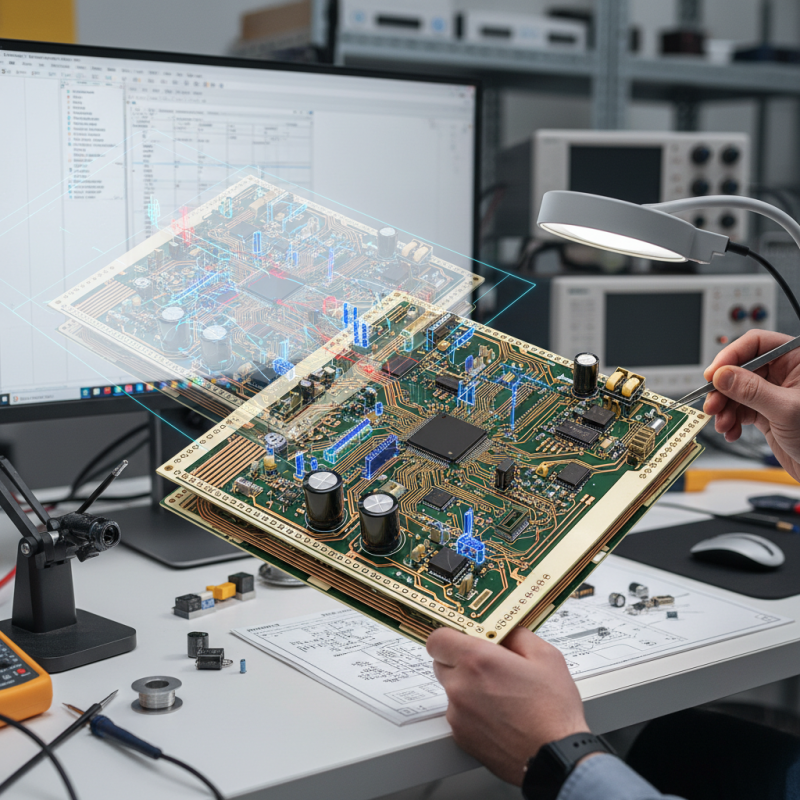
Translating a schematic into a PCB layout can be both exciting and challenging. Begin by understanding the components in your design. Each element on the schematic should correspond to a unique footprint. Ensure you have accurate measurements for each component. If a footprint is too small, it can cause mounting issues. Conversely, a larger footprint may leave too much space.
As you create the layout, remember to consider the placement of traces. Keep them short and avoid sharp angles. Wider traces can handle more current. Be mindful of your ground connections; they need to be solid for reliable performance. Make sure your power supply traces have adequate widths, too. It’s easy to overlook this, but it can lead to voltage drop.
Routing can also present challenges. You might find that your initial layout doesn't fit perfectly. Don't be afraid to adjust as needed. Sometimes, a reworked trace can fix a big issue. It’s beneficial to step back and review your layout periodically. Ask yourself if there are neater connections or better arrangements. Learning from these revisions is crucial for improving your design skills.
How to Design a Printed Circuit Board for Your Electronics Project? - Translating the Schematic into PCB Layout
| Component Name |
Component Type |
Value/Rating |
Footprint |
Quantity |
| Resistor |
Passive |
10k Ohm |
0402 |
5 |
| Capacitor |
Passive |
1uF |
0402 |
3 |
| Diode |
Active |
1N4148 |
DO-35 |
2 |
| Transistor |
Active |
BC547 |
TO-92 |
2 |
| Microcontroller |
Active |
ATmega328 |
TQFP-32 |
1 |
Finalizing and Preparing Your PCB Design for Manufacturing
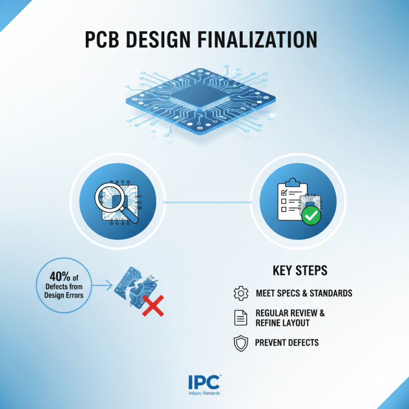
Finalizing your printed circuit board (PCB) design requires careful attention. Ensure your design meets all specifications and industry standards. According to a report by IPC, about 40% of PCB defects arise from design errors. Regularly reviewing and refining your layout is crucial.
Tip: Conduct design rule checks to avoid common pitfalls. Utilize software tools that highlight potential issues. Properly assign component values to prevent confusion during assembly.
Moreover, pay attention to silkscreen layers. They can affect manufacturing and assembly processes. Keep your silkscreen clear of pads and holes. Some engineers overlook this, leading to increased costs and delays. A clean design can save time and money.
Tip: Create a checklist for final reviews. Include aspects like trace widths, hole sizes, and layer stack-up. This will help catch errors before sending your design to production. Remember, precision in this phase can prevent major setbacks later in the project.