How to Design a Printed Circuit Board for Beginners?
Designing a printed circuit board can be an exciting journey. It's a blend of art and science. For beginners, diving into this field may seem daunting at first. However, with a little guidance, anyone can start creating their own designs.
Understanding the basics of a printed circuit board is essential. This includes knowing components, traces, and layouts. Each decision impacts the final functionality. Beginners often feel overwhelmed by all the details. It's normal to make mistakes along the way. Learning from these errors is part of the process.
To design your own printed circuit board, start with simple projects. Choose a basic schematic. Experimentation leads to greater understanding. Don't hesitate to seek help or resources. Connecting with communities can also provide valuable insights. Embrace the challenges; they are stepping stones to mastery.
Understanding the Basics of Printed Circuit Board Design
When diving into printed circuit board (PCB) design, grasping the basics is crucial. A recent report by Statista indicates that the global PCB market is set to reach approximately $80 billion by 2026. This growth highlights the importance of solid design principles. Understanding layers, traces, and components lays the foundation for effective designs. Beginners often overlook these elements, leading to common mistakes.
Understanding the layout is essential for functionality. Most PCBs have multiple layers. Each layer serves a purpose. Mistakes in layer design can lead to circuit failure. According to IPC standards, a well-designed PCB should minimize electromagnetic interference. Beginners need to consider spacing between traces. Insufficient space can cause shorts or signal degradation.
Design software tools can aid learning but may also be overwhelming. Many beginners struggle with these programs. It's vital to invest time in tutorials. Recognizing the complexity of signals and power distribution is important. Neglecting this understanding can result in inefficient designs. Embracing iterative design practices can improve outcomes. Testing and revising designs leads to better products.
Essential Tools and Software for PCB Design Beginners
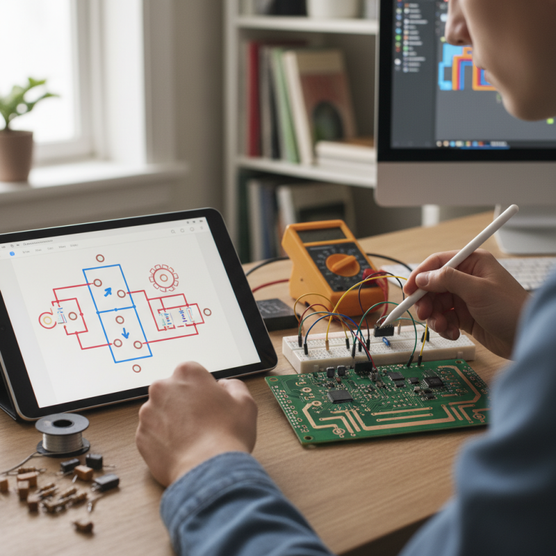
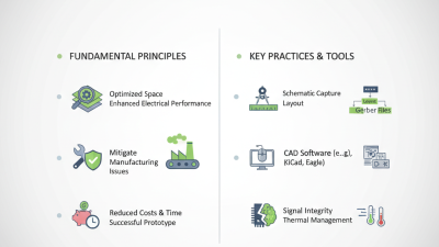
When starting with PCB design, having the right tools is crucial. A basic software suite can make a big difference. Look for options that offer schematic capture and layout capabilities. These features will help you visualize your circuit and layout effectively. Some tools are user-friendly for beginners, but mastering them takes time. Don’t expect to learn everything overnight.
Another essential tool is a reliable breadboard. You can test your circuits before finalizing your PCB. Prototyping on a breadboard allows for easy adjustments. Layout mistakes can happen. Sometimes, components don’t fit as planned. It’s important to adapt and correct them early.
Before printing your PCB, try a simple design first. You'll encounter challenges, like trace routing issues or component placements. These bumps can be frustrating. Reflect on your mistakes; they are part of the learning process. Embrace iterative design. Each revision improves your skills.
Common Pitfalls in PCB Design and How to Avoid Them
When designing a printed circuit board (PCB), common pitfalls can lead to major issues. One critical mistake is neglecting proper component placement. According to a recent industry report, 40% of design errors stem from components being too close or improperly aligned. This can cause interference and circuit failures. Proper spacing is essential, and using guidelines can help.
Another frequent issue is ignoring thermal management. A study revealed that 30% of PCBs fail due to overheating. Designers often underestimate the heat generated by components. Appropriate heat sinks and airflow are crucial for longer-lasting circuits. Skipping simulations in this area can lead to catastrophic results.
Additionally, inadequate documentation can hinder future modifications. Many designers overlook keeping detailed records. An estimated 25% of project delays arise from unclear sketches and notes. Well-organized documentation saves time when revisions are necessary. Embracing these considerations can elevate a beginner's PCB design, although room for improvement always exists.
Finalizing and Preparing Your PCB for Manufacturing
Finalizing and preparing your PCB for manufacturing is an essential step in the design process. Start by double-checking your schematic for any errors. Use software tools to verify connections and component placements. It’s common to overlook small details. A misplaced component can lead to significant issues later.
Next, create a bill of materials (BOM). This document lists all components needed for your PCB. Accuracy is vital here. An incomplete BOM may delay production. You might need to revisit your design if some components are hard to find.
Finally, generate the Gerber files. These files guide the manufacturer in constructing your PCB. Ensure you follow the specific requirements of the fabrication house. Missing information can lead to miscommunication. It’s wise to review everything one last time. Errors at this stage can be costly. Take time to reflect and refine your design for the best outcome.
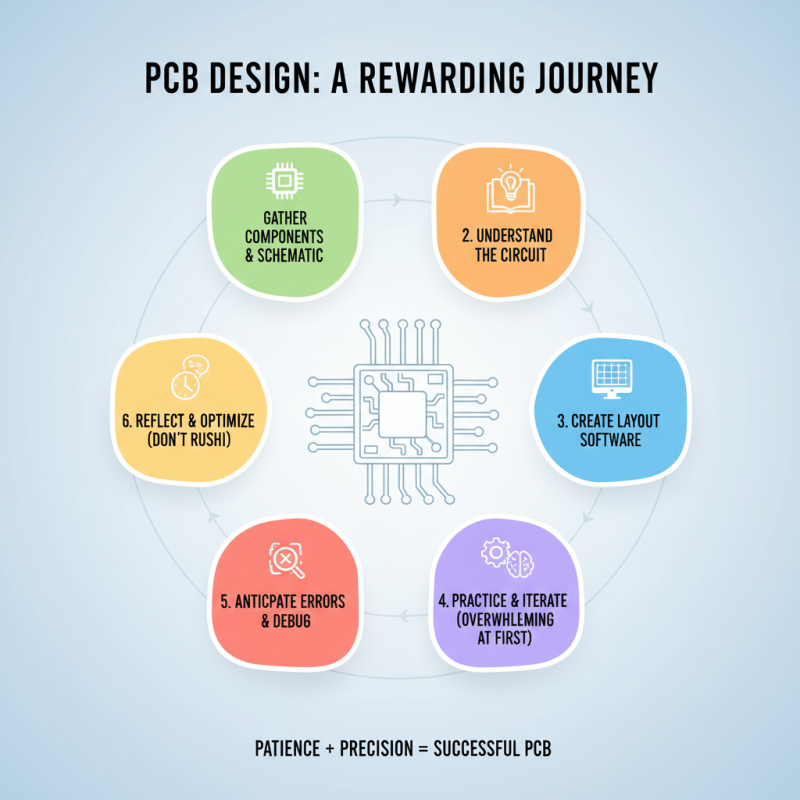
PCB Design Process Steps