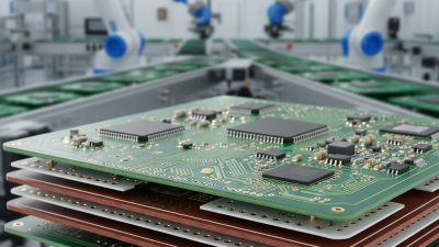
Effective circuit board design is crucial in electronics. A well-designed circuit board can improve performance, reliability, and efficiency. Poor design can lead to failures and increased costs.
When creating a circuit board, several factors should be considered. Components' placement impacts signal integrity and thermal management. Designing for manufacturability is vital. A complex layout may look impressive but can hinder production. Each choice in the design process affects the end product's quality.
Attention to detail is essential in circuit board design. Mistakes can lead to circuit malfunctions. Reviewing designs critically can help identify flaws. Emphasizing practicality while fostering creativity will lead to better designs. Striking this balance is not easy but necessary for success.
Designing an effective circuit board requires careful planning and attention to detail.
Spacing between components is crucial.
Too close, and you might face interference issues. Too far, and signal integrity can suffer.
Aim for optimal distances that prevent crosstalk. It's an art as much as a science.
Consider your layout carefully. Each trace should be as short and direct as possible.
Longer traces can introduce delay and increase resistance.
Use ground planes to minimize noise.
This simple method can enhance performance significantly. Don't overlook thermal management either.
Heat can damage components over time. Ensure there’s enough spacing or cooling mechanisms.
Sometimes, expected heat levels are hard to predict, leading to unexpected problems.
Always review your design before finalizing it.
Mistakes often hide in plain sight.
Missing a connection or misplacing a component can lead to failures.
Use simulation tools to test your layout. They will reveal issues you might have missed.
Honest self-reflection on your design process is key.
Even experienced designers make errors, so never skip this step.
Rethink your designs. Each iteration can lead to improvement.
Layer stack-up is critical in PCB design. A well-structured layer configuration can enhance signal integrity, reduce electromagnetic interference, and improve thermal management. According to a recent industry report, improper layer organization can lead to a 50% increase in signal failure rates. This alarming statistic highlights the necessity of careful planning in layer stack-up.
When designing your PCB, consider these tips:
When designing circuit boards, trace width and spacing are critical for signal integrity. Properly optimizing these factors can significantly reduce attenuation and interference. According to a study by IPC, nearly 50% of PCB failures stem from inadequate trace design. This emphasizes the importance of getting it right.
Consider the standard rule of thumb: wider traces can carry more current, but they also take up valuable space. A trace width of 0.5 mm may suffice for lower currents, but high-power applications often need 1 mm or more. Spacing matters, too. A gap of 0.3 mm is generally safe, but overly close traces can lead to crosstalk and reduce performance.
It's easy to overlook these details. Sometimes, engineers opt for narrower traces to save space. However, this can lead to overheating or signal distortion. Balancing trace width and spacing with the board's overall layout is not straightforward. There's always a trade-off between size, cost, and reliability. Engaging in thorough simulations can help identify potential problems before production.
Effective PCB design is crucial for minimizing electromagnetic interference (EMI). Ground planes play a vital role in this process. A solid ground plane helps with signal integrity. It provides a low-impedance path for return currents. This can significantly reduce noise in sensitive electronic circuits.
When integrating ground planes, consider their placement. They should be strategically located within the PCB layout. Simply adding a ground plane is not always sufficient. Ensure that the ground plane covers potential high-frequency areas. Pay attention to component placement. Avoid long traces that can act as antennas. Keep traces close to the ground for better EMI mitigation.
Think about thermal management as well. Ground planes can help dissipate heat. However, ensure that the ground does not touch sensitive signal paths. This can create unintentional coupling. Testing in real-world conditions is essential. Sometimes, simulation results do not match actual performance. Iterate your design based on practical feedback. Rethink your strategies continually to improve the EMI performance.
When it comes to PCB designs, thermal management is often overlooked. Effective thermal management strategies are crucial for ensuring reliability and performance. Here are some techniques that can enhance your designs.
Consider using thermal vias. These small holes help dissipate heat from the components to the PCB layers. They can be cheap and effective but may require careful placement. Also, try to use copper pours. This increases surface area and improves heat conduction. However, it may complicate the routing process.
Utilizing heat sinks can also be a viable option. They help to draw heat away from critical components. Be sure to check the thermal resistance. Sometimes, heat sinks can be cumbersome and take up valuable board space. Balance is key; you want effective cooling without cluttering your design.
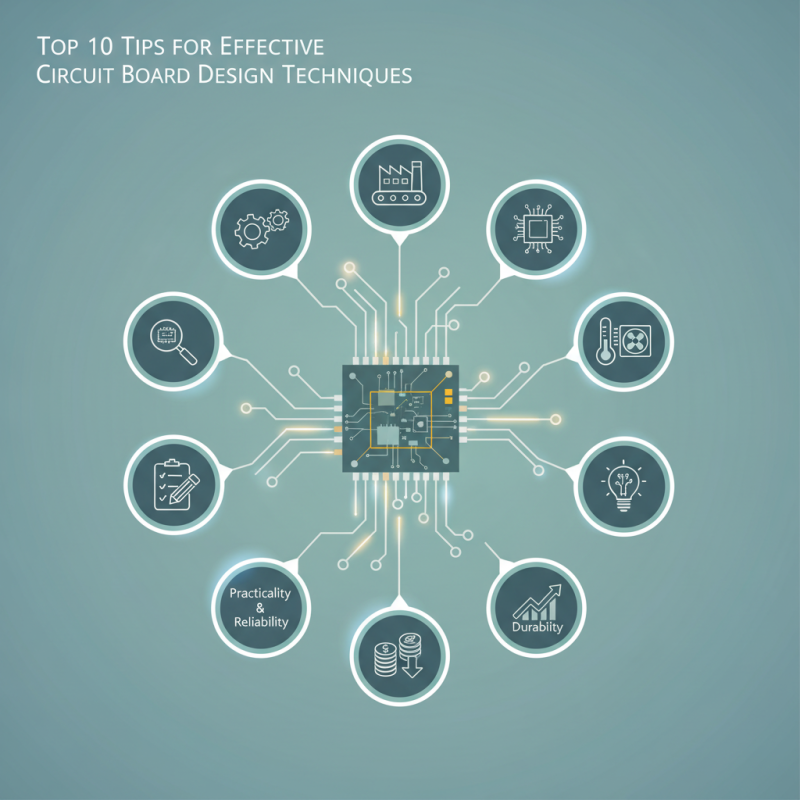
Effective circuit board design is crucial for ensuring reliability and performance in electronic devices. This article outlines top techniques to enhance your PCB design process. Understanding the significance of layer stack-up plays a pivotal role in managing signal integrity, while optimizing trace width and spacing is essential for minimizing electromagnetic interference (EMI). Additionally, utilizing ground planes can significantly reduce EMI effects, improving overall circuit performance.
Thermal management strategies are equally important, as they prevent overheating and ensure longevity of the circuit board. Finally, adhering to design rules compliance and using simulation tools will help verify the reliability of your PCB designs. By incorporating these tips, designers can create more efficient and robust circuit boards that meet the demands of modern electronics.
| Cookie | Duration | Description |
|---|---|---|
| cookielawinfo-checkbox-analytics | 11 months | This cookie is set by GDPR Cookie Consent plugin. The cookie is used to store the user consent for the cookies in the category "Analytics". |
| cookielawinfo-checkbox-functional | 11 months | The cookie is set by GDPR cookie consent to record the user consent for the cookies in the category "Functional". |
| cookielawinfo-checkbox-necessary | 11 months | This cookie is set by GDPR Cookie Consent plugin. The cookies is used to store the user consent for the cookies in the category "Necessary". |
| cookielawinfo-checkbox-others | 11 months | This cookie is set by GDPR Cookie Consent plugin. The cookie is used to store the user consent for the cookies in the category "Other. |
| cookielawinfo-checkbox-performance | 11 months | This cookie is set by GDPR Cookie Consent plugin. The cookie is used to store the user consent for the cookies in the category "Performance". |
| viewed_cookie_policy | 11 months | The cookie is set by the GDPR Cookie Consent plugin and is used to store whether or not user has consented to the use of cookies. It does not store any personal data. |