Essential PCB Design Tips for Beginners to Master?
PCB design is a critical skill for any aspiring electronics designer. Mastering this area can lead to innovative projects and successful products. However, many beginners face common challenges in the design process. Understanding the basics can help mitigate these issues.
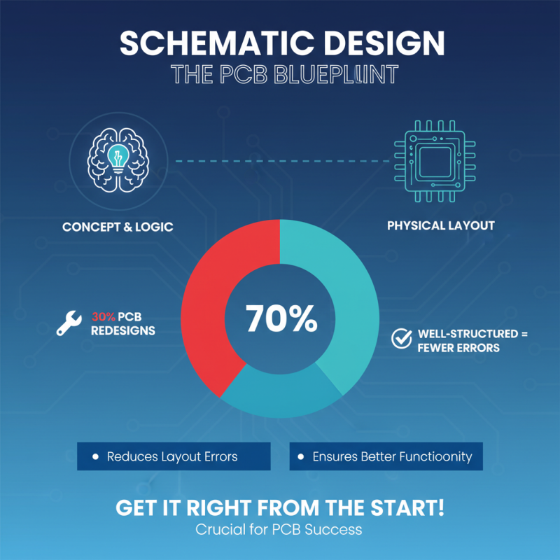
Attention to detail is essential in PCB design. A small mistake can lead to significant problems later on. For example, incorrect component placement may cause connectivity issues. Additionally, beginners often overlook the importance of routing. Your design may look good on paper but fail in practice if routed poorly.
Learning PCB design requires practice and patience. Experiment with different layouts and techniques. Seek feedback from experienced designers. Embrace mistakes as opportunities for growth. Reflect on what works and what doesn’t. The journey of mastering PCB design is filled with challenges, but it is also rewarding.
Essential Considerations for Selecting PCB Materials and Substrates
When selecting PCB materials and substrates, consider several essential factors. The choice of material affects performance, durability, and cost. Common options include FR-4, polyimide, and Rogers. Each has unique properties that cater to different applications. For instance, FR-4 is a popular choice due to its balance of cost and performance. It is widely used in most circuits. However, in high-frequency applications, alternative materials may be needed.
Tips for selecting PCB materials include understanding your project's requirements. Determine the environmental conditions the PCB will face. High temperatures and humid environments can impact the choice of substrate. Also, think about the electrical properties your design requires. Conductivity and dielectric constant are crucial for signal integrity.
It's essential to not overlook the thickness and copper weight. These factors influence the thermal management of your circuit. Thin materials may save space but can lead to overheating. Consider drafting multiple iterations when experimenting with materials. This reflective practice helps identify the best fit for your design. Remember, the right material can make or break your PCB performance.
Key Design Rules: Trace Width, Spacing, and Signal Integrity
When designing a PCB, some essential guidelines revolve around
trace width,
spacing, and
signal integrity.
Trace width affects current capacity.
Wider traces carry more current, which is crucial in power circuits.
However, this could lead to manufacturing issues if not sized correctly.
It’s a balancing act. Too wide can waste space; too narrow could cause overheating.
Spacing is another critical element.
Adequate space between traces prevents short circuits and signal interference.
But what if the space is too wide?
This might affect board real estate.
Signal integrity is paramount,
particularly for high-frequency designs.
Inadequate design can cause noise.
This impacts the overall performance.
Paying attention to these details can make a noticeable difference.
Yet, many beginners overlook them, leading to frustrating revisions.
Remember to validate your design frequently.
Testing can reveal errors early on.
Mistakes often happen in the initial phases.
Adjustments are part of the learning curve. Embrace these challenges.
They help sharpen your skills.
PCB design is not just about following rules. It’s a process of exploration and improvement.
Utilizing Software Tools for Efficient PCB Design and Simulation
When embarking on PCB design, using the right software tools can significantly enhance efficiency. A report by IPC states that effective design tools can reduce project time by up to 40%. These tools allow designers to visualize circuits in real-time, streamlining the process. Moreover, simulation features can predict how a PCB will perform in various conditions. This is crucial for testing theories without physical trial and error.
However, beginners often overlook the learning curve associated with these software packages. Many tools have complicated interfaces. Trying to master them without proper guidance can lead to frustration. A survey revealed that nearly 50% of new designers feel overwhelmed by software complexities. This emphasizes the need for tutorials and support communities. Investment in training can pay off; it can improve design quality and efficiency.
The integration of automation in design tasks is another game-changer. Automated routing features save time by managing layout complexities. Yet, reliance on automation also poses risks. Designers may become passive, neglecting fundamental principles. Feedback from industry veterans suggests balancing tool usage with a strong foundation in manual design skills. Mastering both can lead to more robust PCB designs.
Essential PCB Design Tips for Beginners
This chart displays the user satisfaction ratings for various PCB design software tools commonly used by beginners. Understanding which tools are favored can help new designers choose the right software to facilitate their learning process.
Prototyping Techniques: From Breadboarding to Final PCB Production
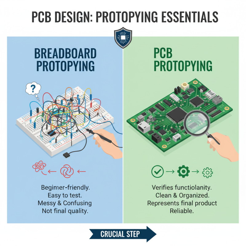
Prototyping is a crucial step in PCB design. It helps verify circuit functionality before moving to production. Breadboarding is a common technique used by beginners. It allows you to test circuits with ease. However, it can lead to messy setups. Wires may cross, causing confusion. This may not reflect final product quality.
A study by PCB Design Magazine indicates that 35% of prototypes fail due to design errors. Many errors go unnoticed during the breadboarding phase. This often leads to delays in the production timeline. Transitioning to a more structured prototyping technique can help. Tools like simulations can identify issues early. They can save time and money in the long run.
After breadboarding, moving to a PCB layout is the next step. This process requires attention to routing, isolation, and component placement. Poorly routed boards can cause signal integrity issues. In fact, 25% of engineers face problems related to signal degradation. Learning to pay attention to these details is essential. Each decision affects the final product's performance. Hence, explore different techniques and learn from mistakes. Each iteration will enhance your design skill.