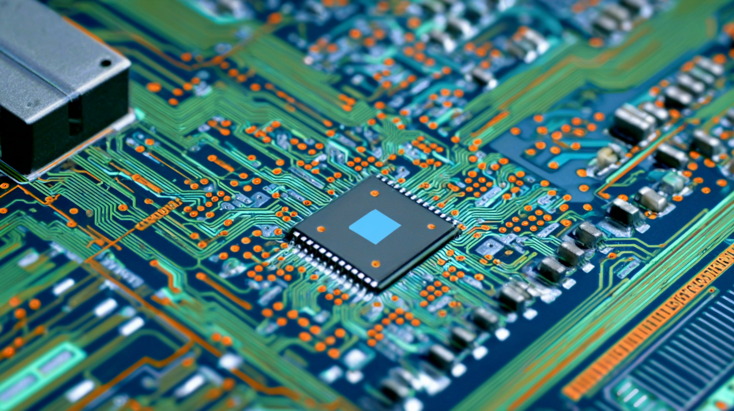
Understanding the Importance of PCB Layout in Modern Electronics Design
 In today's fast-paced world of electronics design, understanding the significance of PCB layout has become essential for creating efficient and reliable devices. A well-executed PCB layout not only enhances the performance of electronic components but also plays a crucial role in minimizing electromagnetic interference and ensuring signal integrity. As devices become increasingly complex, the intricacies involved in designing a PCB layout require designers to adopt best practices and innovative strategies to meet the demanding specifications of modern electronics.
The process of PCB layout encompasses several key considerations, from component placement to trace routing, which directly impact the overall functionality of the electronic circuit. Each decision made during the layout process can affect how signals travel across the board, influence thermal management, and determine the device's manufacturability. Understanding these critical design factors is paramount for engineers who aim to develop cutting-edge technology that meets consumer needs and adheres to industry standards.
As we dive deeper into the nuances of PCB layout, we will explore practical tips and guidelines that can help designers optimize their layouts for performance and reliability. This discussion will provide valuable insights into the best practices that can be employed to ensure that modern electronics designs stand out in an increasingly competitive market.
Essential Principles of PCB Layout Design for Modern Electronics
The evolution of electronics design is heavily influenced by the principles of printed circuit board (PCB) layout, particularly in the context of modern trends such as miniaturization, flexible PCBs, and automotive applications. As electronic devices become smaller and more complex, the demand for efficient PCB layouts has soared. Designers must prioritize correct component placement, optimal routing, and impedance matching to ensure functionality and performance. Understanding how to effectively manage space while adhering to electrical design rules is crucial for achieving reliable and high-performance circuits.
Moreover, the rise of flexible PCBs has introduced new challenges and opportunities in PCB layout design. Designers need to consider mechanical stress, thermal management, and signal integrity while crafting flexible solutions that meet stringent industry standards. As the automotive sector increasingly incorporates electronic components, the principles of PCB layout become even more vital. The integration of various electronics in vehicles, from infotainment systems to advanced driver-assistance systems, calls for meticulous design practices that accommodate both flexibility and robustness. Hence, mastering the essential principles of PCB layout is indispensable for engineers striving to innovate in the rapidly evolving field of electronics.
Understanding the Importance of PCB Layout in Modern Electronics Design - Essential Principles of PCB Layout Design for Modern Electronics
| Principle |
Description |
Impact on Design |
| Layer Stackup |
Choosing the right number of layers based on component density and signal integrity. |
Affects manufacturability and cost of PCB. |
| Trace Width |
Determining width based on current carrying capacity and impedance. |
Ensures reliability and performance of power delivery. |
| Ground Planes |
Utilizing solid ground planes to reduce noise and improve signal integrity. |
Minimizes voltage drop and enhances EMI performance. |
| Component Placement |
Strategic placement to minimize trace lengths and thermal issues. |
Improves performance and maintainability of the board. |
| Via Design |
Selecting appropriate via types and locations for signal routing. |
Affects signal integrity and layers interconnection. |
| Thermal Management |
Incorporating heat sinks and thermal vias to dissipate heat. |
Prevents overheating and extends the lifespan of components. |
Common Mistakes to Avoid in PCB Layout for Enhanced Performance
In modern electronics design, achieving optimal performance heavily relies on meticulous PCB layout. A frequent pitfall to avoid is neglecting the placement of components, which can lead to signal integrity issues and increased electromagnetic interference (EMI). According to a report by IPC, up to 70% of product failures can be attributed to PCB layout errors. It is crucial to strategically position high-frequency components and minimize trace lengths to ensure robust signal paths.
Another common mistake is overlooking the significance of grounding and power distribution. A poor grounding scheme can result in substantial noise, degrading overall performance. The IEEE emphasizes that implementing a solid ground plane can drastically reduce EMI and improve power integrity. Furthermore, ensuring appropriate trace widths is essential for handling current loads without overheating. Research from the IPC highlights that correcting these layout issues can lead to a performance enhancement of up to 30%, showcasing the direct impact of well-executed PCB design in the efficiency of electronic devices.
Best Practices for Optimizing Signal Integrity in PCB Designs
In modern electronics design, optimizing signal integrity within PCB layouts is crucial for the performance and reliability of electronic devices. Signal integrity refers to the quality of the electrical signals as they travel across the circuit, and any disruption can lead to errors, increased electromagnetic interference, and system failures. Following best practices in PCB design can significantly enhance signal integrity.
One essential tip is to minimize the length of critical signal traces. Shorter traces reduce potential inductance and capacitance, which helps to maintain signal fidelity. Additionally, maintaining a consistent width throughout the signal paths can help avoid reflections that may compromise signal quality. Another effective strategy is to utilize ground planes. A solid ground plane beneath signal traces can provide a low-inductance return path and shield against noise, further improving overall signal integrity.
Lastly, careful consideration of component placement can have a profound impact on signal paths. Strategically positioning components to minimize crossing traces and maintaining adequate spacing between high-frequency traces and ground can prevent unwanted coupling. By implementing these best practices, designers can significantly bolster the performance of their PCB designs and ensure the integrity of signal transmission throughout the electronic device.
Utilizing Layout Tools and Software for Effective PCB Development
In modern electronics design, the importance of a well-structured PCB layout cannot be overstated.
Utilizing advanced layout tools and software is crucial for effective development, allowing engineers to simulate and optimize their designs before the manufacturing process. These tools help in visualizing the circuit and ensuring that all components are correctly placed, reducing the likelihood of design errors.
Tip: When choosing PCB layout software, look for features that streamline the design process, such as automated routing and design rule checks. This can significantly save time and improve the reliability of your final product.
Moreover, leveraging powerful software allows for better management of space and component placement, which is essential in complex designs. Modern tools offer intuitive interfaces and a variety of libraries that contribute to faster prototyping while ensuring adherence to electromagnetic compatibility and signal integrity.
Tip: Regularly update your software to access the latest features and capabilities, which can provide new options for layout optimization and improve your overall workflow.
Key Considerations for Thermal Management in PCB Layout Planning
Thermal management is a crucial aspect of PCB layout planning, especially in the context of modern electronics where components operate at increasingly high speeds and power levels. One of the primary considerations is the strategic placement of components to optimize heat dissipation.
High-power devices should be positioned near the edges of the PCB or in areas with better airflow to prevent thermal accumulation. Additionally, using thermal vias can effectively transfer heat from hot components to the inner layers of the board, where it can be spread out and dissipated more efficiently.
Another important factor in thermal management is the selection of appropriate materials and layer stack-up for the PCB. Utilizing materials with high thermal conductivity, such as copper, can significantly enhance heat dissipation. Furthermore, incorporating thermal pads or sinks into the design can aid in managing hotspots effectively. Designers must also consider the routing of traces; wider traces can handle higher current loads and reduce resistive heating, thus playing a vital role in maintaining the integrity of the circuit. By prioritizing these thermal management strategies in PCB layout planning, engineers can enhance performance, reliability, and longevity of electronic devices.