What Are the Key Steps in Effective PCB Design?

What Are the Key Steps in Effective PCB Design?

In today’s fast-paced electronics industry, effective PCB design is crucial. A well-designed printed circuit board (PCB) can significantly impact product performance and reliability. According to a report by IPC, nearly 30% of all device failures are attributed to poor PCB design. This highlights the importance of following best practices in the PCB design process.

Dr. Jessica Mills, a leading expert in PCB design, emphasizes, "Precision and attention to detail in PCB design are essential to prevent costly errors." Her insights underline the importance of employing a meticulous approach during the design phase. A poorly designed PCB can lead to product recalls and financial loss.

Despite advancements in technology, many engineers still overlook foundational steps in PCB design. This can lead to challenges such as signal integrity issues and component placement mistakes. Reflecting on these gaps can help engineers to refine their designs further. Emphasizing quality and thoroughness can elevate the standard of PCB design in the industry.

What Are the Key Steps in Effective PCB Design?

Understanding PCB Design Fundamentals

What Are the Key Steps in Effective PCB Design?

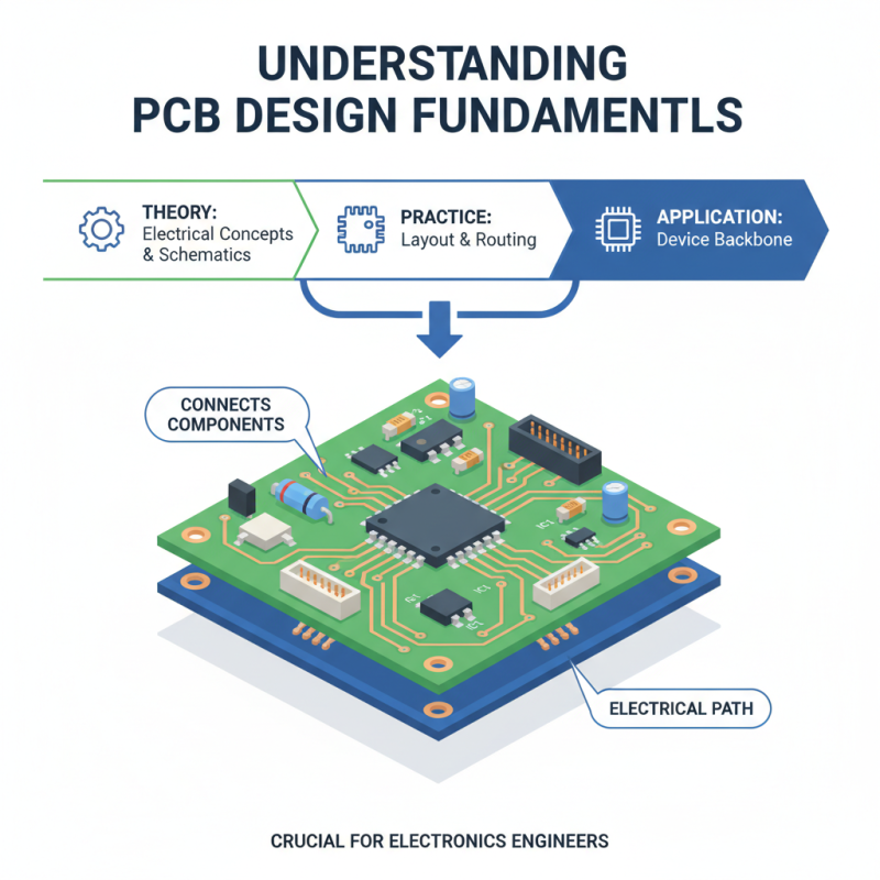
Understanding PCB design fundamentals is crucial for any electronics engineer. A printed circuit board (PCB) serves as the backbone of nearly every electronic device. It connects various components such as resistors, capacitors, and chips, providing a path for electrical current. However, designing an effective PCB involves a deep understanding of both theoretical concepts and practical applications.

Key elements in PCB design include schematic creation, layout planning, and proper component placement. Engineers must ensure that the signal integrity is maintained throughout the design. For example, minimizing the length of traces can help reduce noise. Additionally, thermal management is essential. Poorly designed PCBs may overheat, leading to failures. Balancing these factors often requires experience. Mistakes during the design phase can lead to significant issues later, so careful consideration is vital.

In some cases, designers may overlook the importance of ground planes. A solid ground plane is essential for reducing electromagnetic interference. Additionally, engineers should reassess their workflows regularly. Engaging in peer reviews can uncover hidden flaws. This iterative process is beneficial and can lead to more robust designs. Reflecting on past projects helps identify common pitfalls and improve future designs.

Defining Functional Requirements and Specifications

Defining functional requirements and specifications is crucial in the PCB design process. Clear requirements set the foundation for a successful project. Without them, designers may overlook essential features, leading to costly revisions. The requirements should detail operational performance, environmental conditions, and physical constraints.

It's also vital to engage with cross-disciplinary teams early on. This collaboration helps to identify potential challenges. For example, if thermal management isn't properly defined, overheating might occur, damaging components. Designers often face pressure to meet deadlines, leading to rushed specifications. This can result in overlooked details that affect functionality.

Thorough documentation is essential for ensuring everyone is on the same page. However, keeping it concise is equally important. Long, complex documents can confuse rather than clarify. Frequent revisions allow for refining requirements but can also create inconsistencies. Reflecting on the design process is necessary to adapt and improve future projects.

What Are the Key Steps in Effective PCB Design? - Defining Functional Requirements and Specifications

Step Description Importance Example Tools
1. Define Requirements Gather and specify technical and functional requirements for the PCB. Sets the foundation for design and ensures alignment with user needs. Requirement Analysis Tools
2. Create Schematic Design the circuit schematic based on the defined requirements. Visualizes the circuit and relationships between components. Eda Software (e.g., Eagle, Altium Designer)
3. PCB Layout Design Translate the schematic into a physical layout considering size, space, and routing. Ensures manufacturability and performance efficiency. Layout Tools (e.g., KiCad, CircuitMaker)
4. Design Rule Check (DRC) Verify the design against manufacturer and electrical rules. Reduces errors and ensures compliance before production. DRC Software Features
5. Prototype Testing Create initial prototypes for testing functionality and performance. Identifies potential design flaws before mass production. Prototyping Tools (e.g., breadboards, 3D printers)
6. Final Design Review Conduct a thorough review to finalize design adjustments based on prototype feedback. Ensures readiness for production and optimal performance. Review Checklists and Collaboration Tools

Creating a Schematic Diagram and Component Selection

Creating a schematic diagram is a foundational step in PCB design. It visually represents the circuit and shows the connection between components. Accurate placement of symbols and clear labeling is crucial. Errors at this stage can lead to significant problems later. Each connection must be carefully drawn to avoid confusion.

Component selection is equally important. Engineers must consider specifications like voltage ratings and thermal management. Using the right components ensures optimal performance. Sometimes, it’s tempting to choose the cheapest options, but this can backfire. Reliability and longevity should be top priorities. Overlooking these factors may result in failed prototypes or inefficient designs.

Testing and refining the schematic can reveal hidden flaws. Iterative improvements, based on feedback, can lead to a more robust design. It’s essential to remain flexible during this process. Designing an effective PCB is a journey of continual learning and adaptation.

Developing PCB Layout and Routing Strategies

In developing PCB layout and routing strategies, several critical steps must be taken to ensure effectiveness. Accurate component placement is foundational. It affects signal integrity, thermal performance, and manufacturability. According to a recent industry report, incorrect placement can lead to a 30% increase in production costs due to rework. Understanding the purpose of each component makes placement decisions clearer.

Next, routing strategies should prioritize short, direct paths. This minimizes inductance and capacitance, which can degrade signal quality. A study found that 45% of design failures stem from poor routing techniques. Designers often overlook the impact of ground planes. A solid ground plane can significantly reduce electromagnetic interference, enhancing performance.

Designing for testability is often underestimated. Including test points can simplify troubleshooting later. However, many designs neglect this aspect. Regular feedback from production teams can highlight common issues during assembly. Learning from these experiences can improve future designs, making iterations faster and more effective. Emphasizing these strategies can lead to better performance and lower costs.

Key Steps in Effective PCB Design

Testing and Validation of PCB Designs

Testing and validation are critical steps in PCB design. According to a 2023 industry report by IPC, nearly 40% of PCB failures stem from design flaws. This statistic underscores the importance of thorough testing. Simulations and prototypes should be evaluated under various conditions. This helps identify potential issues early in the design process.

Functional testing is essential. It checks if each PCB performs as expected in real-world scenarios. Additionally, thermal testing assesses how heat affects performance. Data from industry studies indicate that 30% of malfunctions relate to overheating. Regular inspections during production can also ensure quality. However, these measures often reveal more problems than anticipated, prompting further revisions that may slow down the timeline.

Failing to adhere to a structured validation process can lead to costly redesigns. For instance, a single late-stage defect can cause delays of weeks or even months. Addressing these flaws post-production is not only expensive but can damage reputations. Hence, dedicating time for thorough testing and validation becomes an investment in reliability and quality.