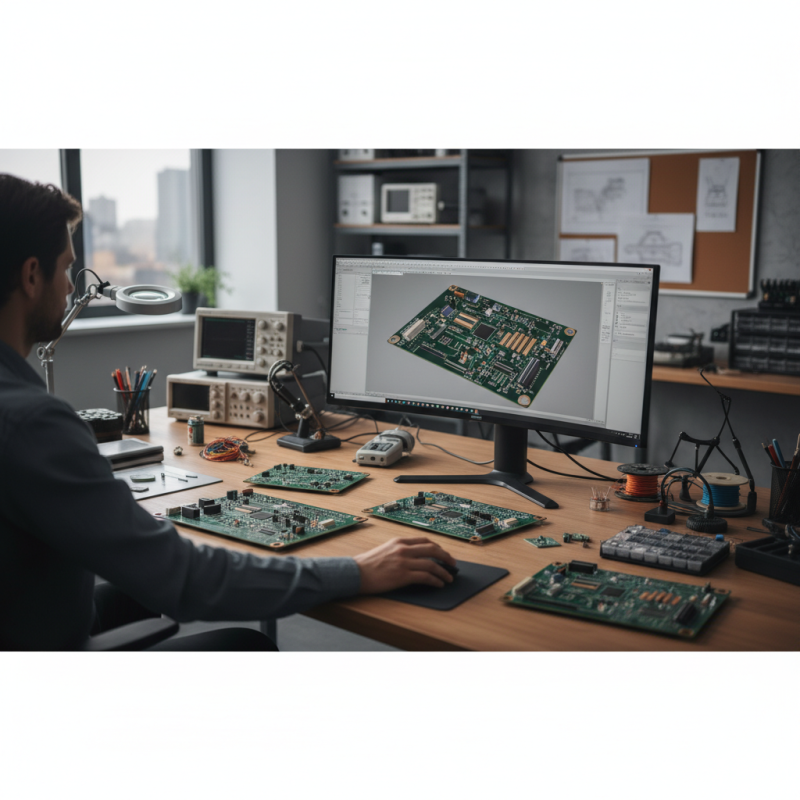
In the ever-evolving world of electronics, mastering PCB board design is a crucial skill for engineers and hobbyists alike. According to Dr. Jane Smith, a renowned expert in electronics engineering, "Effective PCB board design is not just about creating circuits; it's about anticipating future challenges and ensuring reliability and performance." This perspective highlights the importance of not only understanding the fundamentals of PCB design but also applying best practices to stay ahead in a competitive field.
The complexity of modern electronics demands that designers possess a deep knowledge of PCB board design principles, from selecting the right materials to implementing cost-effective manufacturing processes. With the rise of smart devices and IoT applications, having a solid foundation in PCB design is essential for bringing innovative ideas to life. In this article, we will explore essential tips and strategies for mastering PCB board design, helping you to create efficient and effective layouts that can withstand the test of time and technology. By leveraging the insights shared by industry experts, you can enhance your skills and approach design challenges with confidence.

Understanding the fundamentals of PCB (Printed Circuit Board) design is crucial for creating effective and efficient electronic devices. A well-designed PCB not only minimizes manufacturing costs but also enhances the performance and reliability of the final product. According to a report by Research and Markets, the global PCB market is projected to reach $73.7 billion by 2027, emphasizing the importance of mastering PCB design techniques. Understanding the basic elements such as layers, traces, vias, and component placement is the foundation of achieving a successful design.
One essential tip for effective PCB design is to plan your layout carefully. This involves not only the physical arrangement of components but also the routing of traces. Maintaining short, direct paths between components can significantly reduce electromagnetic interference, which is crucial for high-frequency applications. Additionally, consider the thermal management of your design; inadequate heat dissipation can lead to component failure and reduced performance. Comprehensive thermal analysis in the early design phases can prevent costly revisions later.
Another critical aspect is to follow design rules and standards meticulously. Utilizing design rule check (DRC) tools during the design phase helps in identifying potential issues such as trace width violations, spacing problems, and layer stack-up inconsistencies. Implementing these checks can ultimately save time and resources, ensuring a smoother transition from prototype to production. Regularly updating your knowledge about industry standards, as indicated by IPC guidelines, can help ensure compliance and enhance the quality of your boards.
When it comes to mastering PCB board design, selecting the right tools and software is pivotal for efficient layout and simulation. According to the IPC (Association Connecting Electronics Industries), a robust PCB design process can reduce the time to market by as much as 20%. This highlights the importance of using advanced tools that facilitate precise design, allowing engineers to focus on innovation rather than repetitive tasks.
Several tools that stand out in the industry include schematic capture software, PCB layout design tools, and simulation platforms. Software such as circuit simulation tools enables designers to predict how circuits will behave in real-world conditions, thereby minimizing errors and reducing costs. Recent industry reports suggest that companies utilizing comprehensive PCB design software report a 30% reduction in prototyping costs, emphasizing the long-term financial benefits of investing in quality design tools. Furthermore, simulation capabilities provided by certain software allow for thermal and electrical analysis, ensuring that the design meets necessary regulatory requirements before fabrication.
Incorporating a streamlined design workflow involves not only software but also methodologies such as Design for Manufacturability (DFM) and Design for Testability (DFT). Studies indicate that incorporating these principles during the design phase can lead to up to a 25% decrease in manufacturing issues and potential redesign costs. By leveraging the right tools in conjunction with best practices, engineers can achieve optimal results in PCB design, driving innovation and efficiency in the electronics industry.
When embarking on PCB board design, one of the fundamental aspects is the schematic design and component selection. A well-structured schematic not only serves as the blueprint for your circuit but also minimizes potential errors during the layout phase. Start by using clear symbols and annotations, ensuring that each component's purpose is obvious. This clarity not only aids in your current project but also simplifies modifications and troubleshooting in the future.
In terms of component selection, it's vital to consider both functionality and availability. Opt for components that are commonly used to guarantee easy sourcing and support. Be mindful of tolerances, voltage ratings, and package sizes to save time during production and assembly.

When optimizing PCB layout and signal integrity, several core techniques can significantly enhance the performance of your design. One crucial aspect is ensuring proper grounding and power distribution. A well-planned ground plane can greatly reduce electromagnetic interference (EMI) and improve overall signal integrity. According to industry reports, nearly 70% of PCB-related issues stem from poor grounding practices, making this a primary focus area for designers. Utilizing polygon pours for ground connections in multilayer PCBs can help maintain consistent impedance levels across different signal paths.
Another essential technique involves minimizing trace length and utilizing controlled impedance for high-speed signals. Long traces can introduce unwanted capacitance and inductance, leading to signal degradation. Research indicates that signal integrity problems can arise when trace lengths exceed 1/10th of the wavelength of the highest frequency component. Therefore, keeping traces short—preferably under 6 inches for high-frequency signals—and matching the trace impedance to the characteristics of the PCB material can mitigate these issues. Additionally, incorporating vias strategically can help route signals more efficiently while minimizing crosstalk and maintaining a clean signal path.
Moreover, maintaining a proper distance between traces is vital for avoiding interference. A general guideline is to keep adjacent traces at least three times their width apart to minimize capacitive coupling. Advanced modeling tools can assist in predicting and simulating signal behavior in your PCB design. With the right techniques, designers can create high-performance circuits that achieve excellent signal integrity levels, as supported by findings in the IPC-2221 standards, which outline best practices for electronic circuit board design.
Testing and iterating your PCB design is crucial for ensuring reliability and performance, especially as the complexity of electronic devices increases. According to a report by IPC, nearly 60% of PCB failures can be traced back to design errors. Therefore, systematic testing throughout the design process can significantly reduce the risk of costly failures after manufacturing. Utilizing simulation tools to conduct electrical and thermal tests can help identify potential issues early in the design phase. These tools allow designers to visualize how signals will behave under different conditions, enabling them to make necessary adjustments before moving to production.
Iteration is equally important in PCB design. A study published in the Journal of Electronic Materials highlights that iterative design processes can enhance product performance and reduce time-to-market by up to 25%. By engaging in thorough PCB layouts, followed by reviewing and tweaking each version based on testing outcomes, engineers can refine their designs for optimal functionality. Regular feedback loops between design and testing not only improve the reliability of the final product but also enable teams to innovate and incorporate new technologies gracefully. Ensuring robust testing and iteration practices can be a game-changer in delivering high-quality PCBs that meet the demands of today's fast-evolving electronics market.


| Cookie | Duration | Description |
|---|---|---|
| cookielawinfo-checkbox-analytics | 11 months | This cookie is set by GDPR Cookie Consent plugin. The cookie is used to store the user consent for the cookies in the category "Analytics". |
| cookielawinfo-checkbox-functional | 11 months | The cookie is set by GDPR cookie consent to record the user consent for the cookies in the category "Functional". |
| cookielawinfo-checkbox-necessary | 11 months | This cookie is set by GDPR Cookie Consent plugin. The cookies is used to store the user consent for the cookies in the category "Necessary". |
| cookielawinfo-checkbox-others | 11 months | This cookie is set by GDPR Cookie Consent plugin. The cookie is used to store the user consent for the cookies in the category "Other. |
| cookielawinfo-checkbox-performance | 11 months | This cookie is set by GDPR Cookie Consent plugin. The cookie is used to store the user consent for the cookies in the category "Performance". |
| viewed_cookie_policy | 11 months | The cookie is set by the GDPR Cookie Consent plugin and is used to store whether or not user has consented to the use of cookies. It does not store any personal data. |