How to Design PCB Boards for Beginners Tips and Best Practices
The field of electronics is rapidly evolving, with an increasing demand for efficient and innovative designs. The process of PCB board design is fundamental to this evolution, serving as the backbone of countless electronic devices ranging from everyday gadgets to complex industrial machinery. According to a report by MarketsandMarkets, the global printed circuit board (PCB) market is projected to reach USD 90.9 billion by 2025, growing at a CAGR of 3.2% from 2020. This growth emphasizes the critical role that well-designed PCBs play in ensuring performance, reliability, and functionality in electronic applications.
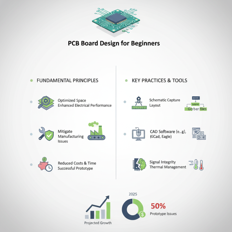
For beginners venturing into PCB board design, understanding the foundational principles and best practices is essential. Effective PCB design not only optimizes space and enhances electrical performance but also mitigates potential manufacturing issues. As highlighted in a study by IPC, nearly 50% of PCB prototypes encounter significant issues during the production phase due to inadequate design practices. Therefore, adopting sound design techniques from the outset is crucial for reducing costs, saving time, and increasing the chances of a successful prototype.
By exploring important concepts, tools, and techniques in PCB board design, newcomers can enhance their skills and contribute to the burgeoning electronics industry. This guide aims to provide valuable insights and practical tips to help beginners navigate the complexities of PCB design, ensuring their projects stand out in a competitive market.
Understanding the Basics of PCB Design for Beginners
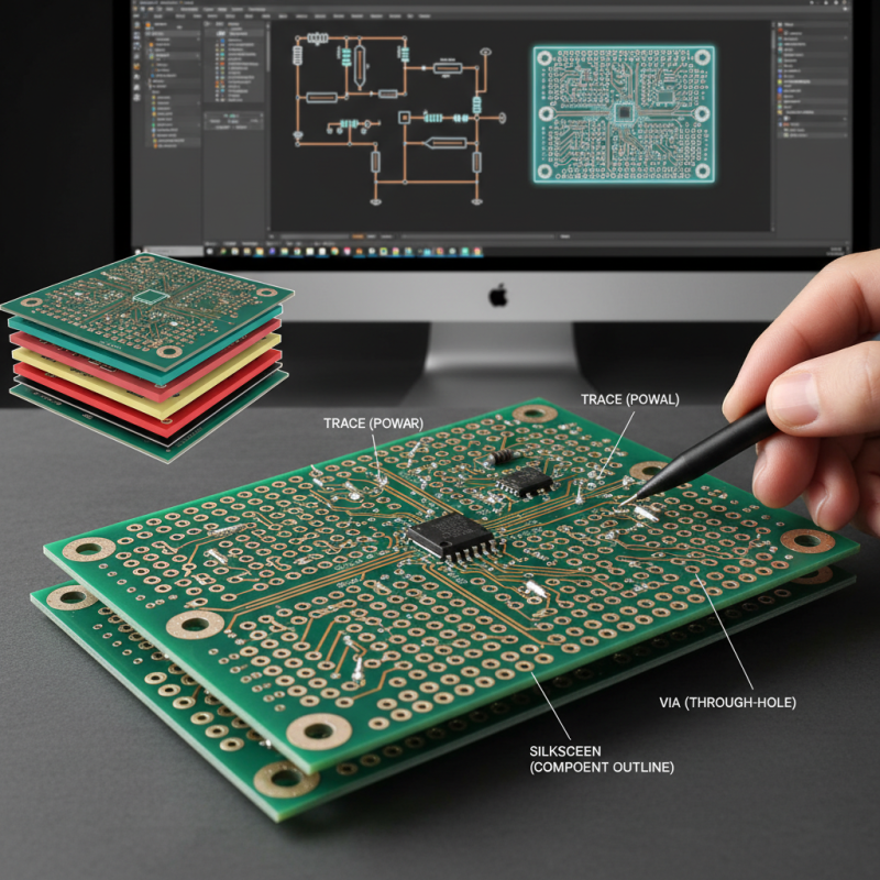
Understanding the basics of PCB (Printed Circuit Board) design is essential for beginners looking to venture into electronics development. PCB design involves translating your electronic circuit schematic into a physical layout that can be manufactured. The first step is to familiarize yourself with fundamental concepts, such as the role of traces, pads, and vias, and how they connect various components on the board. Knowing how to choose the right materials and understanding layer configurations can also significantly impact the board's performance and durability.
Once you grasp these concepts, you can start utilizing PCB design software, which offer tools for creating and modifying your layout. It’s important to practice organizing the components logically to minimize space and maintain signal integrity. Beginners should also learn about design rules, such as clearance and trace width, to ensure their boards will be manufacturable. By adhering to best practices like proper grounding techniques and thermal management, new designers will be better equipped to create efficient and functional PCBs for their projects.
Essential Tools and Software for PCB Layout Creation
When embarking on the journey of PCB design, having the right tools and software is essential for both beginners and experienced designers. The first step is to choose a suitable software platform that provides the necessary features for layout creation and simulation. Look for programs that offer intuitive interfaces and comprehensive libraries of components, allowing new users to familiarize themselves with the design process without feeling overwhelmed. Additionally, integrated simulation tools can help identify potential circuit issues early in the design phase, saving time and effort in the long run.
Essential tools for PCB design also include schematic capture software, which allows designers to create a visual representation of the circuit diagram. This software aids in organizing components and their interconnections, streamlining the transition from schematic to PCB layout. Furthermore, having access to simulation and analysis tools enhances the design process by enabling virtual testing of the PCB functionality. As design complexity increases, these tools become invaluable in ensuring that the final product meets performance and reliability standards before physical manufacturing begins.
Step-by-Step Guide to Schematic Design in PCB
Designing PCB boards starts with a solid schematic, which is the blueprint for your circuit. A well-structured schematic can significantly reduce debugging time and increase the reliability of the design. According to industry reports, up to 60% of development time in electronics can be attributed to troubleshooting and fixing errors that could have been avoided with a clear schematic design. Utilizing intuitive software tools can streamline this process, allowing beginners to visualize their circuits effortlessly.
**Tips:** Start your schematic design by laying out the components you plan to use. Keep in mind that closer proximity between components can reduce the potential for interference and signal integrity issues. Additionally, labeling your components clearly will aid in avoiding confusion down the line, particularly when you move into PCB layout.
As you create your schematic, it's crucial to adhere to best practices by employing a hierarchical structure. This approach not only improves clarity but also makes it easier to manage complex designs—especially critical for multitasking in environments with numerous components. According to a survey from PCB design professionals, 75% stated that having a structured schematic allowed for quicker revisions and an overall smoother design process. This method will help cement a solid foundation for your PCB design journey.
PCB Board Design Complexity by Year
Tips for Effective PCB Layout and Component Placement
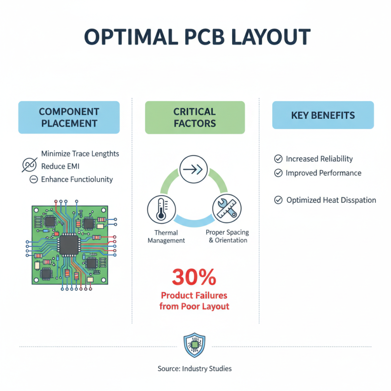
When designing PCB boards, the layout and component placement play pivotal roles in the performance and reliability of the final product. Effective PCB layout involves strategic positioning of components to minimize trace lengths, reduce electromagnetic interference, and enhance overall circuit functionality. According to industry studies, up to 30% of electronic product failures can be traced back to poor PCB layout decisions. Therefore, prioritizing proper spacing and orientation can be critical for optimizing signal integrity and thermal management.
One effective practice is to group related components together. This not only simplifies the connection paths but also aids in reducing parasitic inductance and capacitance, which can greatly impact high-speed circuits. Research from the IPC Association suggests that implementing a structured approach, such as following the "Placement-first" methodology, can significantly improve assembly efficiency and reduce production costs by as much as 20%. Moreover, careful consideration of the power distribution network is essential; utilizing wider traces for power paths and implementing decoupling capacitors close to ICs can help maintain voltage stability and mitigate noise issues.
Additionally, incorporating design for manufacturability (DFM) principles during the component placement phase can lead to smoother manufacturing processes. According to statistical analysis, designs that follow DFM guidelines often result in a 15% reduction in prototype iteration cycles. Such efficiencies not only save time but also enable quicker time-to-market for new devices, underscoring the importance of thoughtful PCB design and layout strategies for beginners aiming to enter the electronics field.
Best Practices for PCB Fabrication and Assembly
When designing PCBs (Printed Circuit Boards), understanding the best practices for fabrication and assembly is crucial for ensuring functionality and reliability. One key aspect is selecting appropriate materials and finishes. The choice of substrate can significantly affect both the performance and manufacturability of the PCB. FR-4 is a commonly used material due to its excellent insulation properties and cost-effectiveness, while other materials may be more suitable for high-frequency applications. Moreover, surface finishes such as ENIG or HASL play an essential role in solderability and resistance to oxidation, influencing the longevity of the connections.
Another important practice involves designing for manufacturability. This means considering the capabilities of PCB fabrication and assembly processes during the design phase. Maintain adequate spacing between traces to avoid issues with routing and ensure that components can be easily placed and soldered. Utilizing standard component sizes and footprints will facilitate assembly and also minimize costs. Additionally, incorporating test points into the design allows for easier troubleshooting and quality assurance in the testing phase, further enhancing the reliability of the finished product. By adhering to these best practices, beginners can foster a smoother design and production process, leading to more effective PCB outcomes.
How to Design PCB Boards for Beginners Tips and Best Practices
| Best Practices |
Description |
| Component Placement |
Arrange components logically to minimize trace lengths and maximize signal integrity. |
| Layer Stackup |
Choose the right number of layers based on complexity and design requirements. |
| Grounding and Power Distribution |
Use a ground plane to reduce noise and ensure stable power distribution. |
| Trace Width Calculations |
Calculate trace widths based on current requirements to prevent overheating. |
| Via Management |
Minimize the number of vias, and ensure they are appropriately sized for current flow. |
| Design for Manufacturability (DFM) |
Follow DFM guidelines to ease assembly and reduce production costs. |
| Thermal Management |
Include thermal relief areas and consider heat sinks for components that produce heat. |
| Testing Points |
Designate test points for easy access to signals for debugging and analysis. |