PCB Design Tips for Beginners to Create Efficient Circuits and Reduce Errors
In the realm of electronics, the importance of effective PCB design cannot be overstated. As a foundational aspect of circuit development, printed circuit boards (PCBs) serve as the blueprint for connecting electronic components. For beginners in this field, understanding the nuances of PCB design can significantly impact the efficiency and reliability of the final product. This article aims to provide essential tips and guidelines that novice designers can follow to enhance their PCB design skills, diminish the risk of errors, and ultimately create more efficient circuits.
With the rapid advancement of technology and the increasing complexity of electronic devices, mastering the principles of PCB design is crucial for those looking to succeed in this competitive industry. From initial schematic layout to the final stages of fabrication, every step in the PCB design process presents an opportunity to optimize performance and streamline production. By embracing proven techniques and common best practices, beginners can lay a strong foundation for their projects, leading to improved functionality and reduced troubleshooting down the line. In this guide, we will explore practical strategies to help upcoming designers navigate the intricacies of PCB design, ensuring that their circuits are not only viable but also efficient and robust.

Understanding the Basics of PCB Design for Beginners
Understanding the basics of PCB design is crucial for beginners aiming to create efficient circuits and minimize errors. According to a report by IPC, the global electronics manufacturing industry is projected to reach $2.6 trillion by 2025. As the demand for precision in electronic devices increases, mastering PCB design becomes essential. A well-designed PCB can lead to improved performance, reduced electromagnetic interference, and lower manufacturing costs.
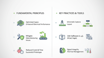
Beginners should start by familiarizing themselves with fundamental concepts such as schematic capture, layout design, and routing techniques. It’s important to understand the significance of component placement and trace width, as improper design choices can lead to issues like signal degradation or overheating. Data from research by the IEEE indicates that nearly 30% of PCB failures are due to design errors. By adopting best practices such as proper grounding and the use of design rule checks (DRCs), beginners can significantly enhance the reliability of their circuits. Furthermore, leveraging simulation tools can help in visualizing circuit behavior before production, ultimately saving time and resources.
PCB Design Tips for Beginners: Component Placement Efficiency
Essential Tools and Software for PCB Circuit Design
When venturing into PCB design, understanding the essential tools and software is crucial for beginners aiming to create efficient circuits and minimize errors. According to a recent report by industry specialists, nearly 60% of design engineers cite their primary challenges as design verification and layout optimization. This highlights the importance of employing software that assists in automating assessments and simplifying the design workflow.
Commonly used tools include schematic capture, PCB layout applications, and simulation software. These tools not only streamline the process but also enhance accuracy by allowing engineers to visualize the circuit performance under various conditions. A study showed that using advanced schematic capture software can reduce layout errors by up to 30%, significantly lowering prototyping costs and development time. Furthermore, simulation tools enable designers to anticipate potential issues such as signal integrity and power distribution, ensuring that the final product is reliable.
Moreover, with the increasing complexity of electronic devices, software that supports multi-layer designs, real-time collaboration, and integrated design rule checks is becoming essential. Research indicates that teams utilizing comprehensive PCB design suites experience a 25% increase in productivity compared to those using basic tools. Embracing these essential tools not only aids in crafting high-quality PCBs but also fosters a more efficient and error-free design environment.
Key Principles of Designing Efficient Circuits
When designing printed circuit boards (PCBs), understanding the key principles of creating efficient circuits is essential for minimizing errors and optimizing performance. One fundamental principle is to maintain a clear layout that prioritizes signal integrity and minimizes interference. This involves strategic placement of components to shorten trace lengths, which effectively reduces inductance and capacitance issues. Keeping critical signal paths direct and free from unnecessary bends will not only enhance the performance of the circuit but also simplify debugging and modifications in the future.
Another vital principle is the use of appropriate grounding techniques to ensure stability and reduce noise. A solid ground plane can serve as an effective sink for noise, which is particularly important in circuits sensitive to electromagnetic interference. Additionally, employing proper decoupling techniques, such as placing capacitors close to power pins of ICs, can help in maintaining consistent power delivery and reducing voltage spikes.
By adhering to these principles, beginners can create efficient PCB layouts that are less prone to errors, ultimately leading to more reliable circuits.
Common Errors in PCB Design and How to Avoid Them
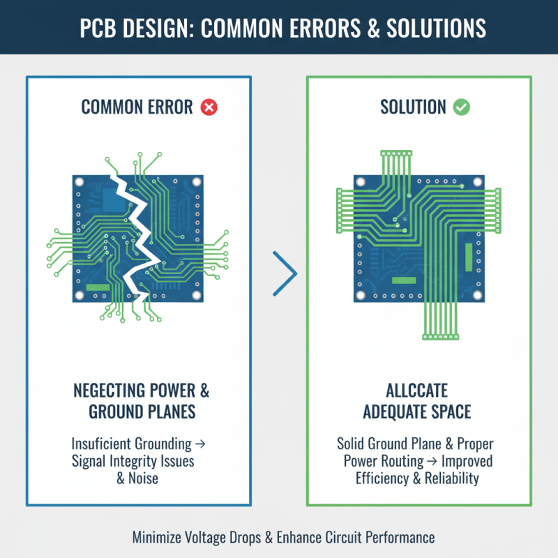
In PCB design, avoiding common errors can significantly improve the efficiency and reliability of circuits. One prevalent mistake is neglecting the power and ground plane. Insufficient grounding can lead to signal integrity issues and increased noise, which might affect the overall performance of the circuit. To mitigate this, designers should allocate adequate space for a solid ground plane and ensure proper routing of power supply traces to minimize voltage drops.
Another frequent error involves improper component placement and routing. Overlooking the arrangement of components can lead to longer signal paths, which may introduce unwanted delay and crosstalk. It is vital to consider both the functionality and manufacturability of the layout. Keeping high-frequency components close together and minimizing trace length enhances performance. Additionally, utilizing design rule checks (DRCs) can help catch potential errors early in the design process, ensuring that the PCB functions as intended before moving to production.
Best Practices for Testing and Iterating PCB Designs
Testing and iterating PCB designs is a crucial phase in the development of efficient and reliable circuits. According to a report by IPC, nearly 70% of PCB design issues stem from poor testing and validation processes. This statistic highlights the importance of dedicating adequate time and resources to test designs thoroughly before final production. One recommended approach is to adopt simulation tools that allow engineers to visualize circuit behavior under varying conditions, addressing potential issues early in the design process. For instance, thermal simulations can prevent overheating problems, which is essential as components become denser in modern designs.
Iterative testing, where designs are modified based on test results, can significantly reduce the number of errors in final products. A survey by TechValidate found that companies implementing iterative design processes reported a 40% reduction in time-to-market due to fewer design revisions in later stages. Early prototyping using low-fidelity models can also provide valuable insights, allowing teams to experiment and refine their designs without substantial cost. Combining simulation, iterative testing, and early prototyping creates a robust strategy that minimizes risks and enhances the overall quality of PCB designs, leading to greater innovation and efficiency in electronic products.
PCB Design Tips for Beginners to Create Efficient Circuits and Reduce Errors
| Tip |
Description |
Benefits |
| Start with a Clear Schematic |
Create a detailed schematic before moving to PCB layout to ensure all components are correctly represented. |
Reduces errors in the layout phase and saves time in debugging. |
| Choose the Right Footprint |
Select component footprints that match the actual components used to avoid fitting issues on the PCB. |
Ensures proper fitting and reduces component placement errors. |
| Keep Trace Lengths Short |
Minimize the length of traces to reduce inductance and resistance. |
Enhances performance and signal integrity of the circuit. |
| Use Ground Planes |
Utilize ground planes to provide a low-resistance path for return currents. |
Improves overall stability and reduces electromagnetic interference. |
| Test Iteratively |
Conduct tests at various stages of development to catch issues early. |
Reduces time and costs associated with late-stage redesigns. |