Ultimate Guide to PCB Design Trends in 2025 for Electronics Enthusiasts
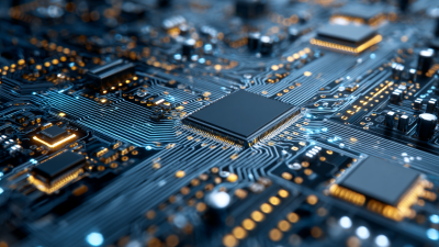
In the rapidly evolving world of electronics, staying ahead of the curve is essential for enthusiasts and professionals alike. As we approach 2025, understanding the emerging trends in PCB design becomes crucial for anyone involved in the field. The realm of PCB design is not only about creating efficient circuit boards; it encompasses a wide range of innovations that enhance functionality, improve manufacturability, and reduce costs. This ultimate guide aims to illuminate the pivotal PCB design trends set to shape the industry in the near future.
From advancements in materials to the integration of smarter design software, the landscape of PCB design is undergoing remarkable changes. Topics such as increasing miniaturization, sustainability efforts, and the rise of automation will be explored, helping enthusiasts adapt their skills and knowledge to meet the demands of modern electronics. Whether you're a seasoned professional or a hobbyist, understanding these trends will not only provide valuable insights but also inspire fresh ideas for your upcoming projects. Join us as we delve into the exciting future of PCB design, revealing what lies ahead for electronics enthusiasts in 2025 and beyond.

Emerging PCB Materials: Enhancing Performance and Sustainability in 2025
As the electronics industry continues to evolve, the selection of materials used in printed circuit boards (PCBs) is becoming increasingly critical. In 2025, there is a notable shift towards advanced materials that not only enhance performance but also promote sustainability. Emerging materials such as biodegradable substrates and recycled composites are gaining traction, offering manufacturers a way to reduce their environmental footprint. These innovative materials facilitate lower energy consumption during production and improve the recyclability of electronic products post-consumer use.
In addition to sustainability, new materials are directly contributing to improved performance characteristics. High-frequency laminates and low-loss dielectric materials are being adopted to meet the demands of faster electronics, essential for applications like 5G communication and IoT devices. Furthermore, advances in thermal management materials are helping to address heat dissipation challenges that arise in compact and high-performance designs. As these materials continue to evolve, manufacturers are likely to witness enhanced durability, reliability, and overall efficiency in their PCB designs, making them a crucial focus for electronics enthusiasts and professionals alike.
Emerging PCB Material Trends in 2025
Advanced Design Techniques: Leveraging AI and Machine Learning in PCB Layout
As we look towards 2025, the integration of artificial intelligence and machine learning in PCB design is set to revolutionize the electronics industry. Advanced design techniques utilizing AI can significantly optimize layouts, improving both efficiency and performance. According to a recent industry report by Technavio, the global market for AI in electronics is expected to grow by over 30% annually, reaching a value of $17 billion by 2025. This growth is driven by the increasing complexity of electronic devices and the demand for faster design cycles.
Incorporating machine learning algorithms allows designers to predict potential issues before they arise, reducing the need for extensive prototyping. By analyzing historical data, AI can identify optimal routing paths and component placements that minimize interference and enhance thermal performance. For electronics enthusiasts looking to stay ahead, leveraging these advanced tools can lead to innovative designs that push the limits of current technology.
Tip: To effectively implement AI in your PCB design, start by collecting and organizing historical design data. This will not only help train your machine-learning algorithms but also enable you to identify patterns that can inform better decision-making in future projects.
As PCB layouts become more intricate, the use of AI helps streamline the design process, making it easier to manage what would be overwhelming complexity. Using generative design techniques powered by AI, designers can explore numerous configurations quickly, finding the best possible solutions that align with both performance and manufacturability requirements.
Tip: When adopting machine learning tools, ensure your team is well-versed in the basics of data science. This foundational knowledge will empower you to fully leverage AI capabilities in your PCB design processes.
Miniaturization Trends: Addressing Space Constraints in Modern Electronics
The trend of miniaturization in PCB design has become a crucial focus for engineers and electronics enthusiasts alike as devices continue to shrink in size and increase in functionality. Modern electronics face significant space constraints, driven by the demand for portable and compact solutions. This evolution requires innovative approaches to component placement, circuit design, and manufacturing techniques. By employing advanced technologies like surface mount technology (SMT) and densely packed multilayer PCBs, designers can maximize space utilization while ensuring optimal performance and reliability.
Furthermore, as the Internet of Things (IoT) and wearable devices gain traction, the need for smaller, more efficient PCBs becomes imperative. Designers are exploring new materials and fabrication methods that allow for thinner, lighter boards without compromising electrical performance. Techniques such as additive manufacturing and integrated passive components help to streamline designs and reduce overall physical footprint. Addressing space constraints not only enhances product functionality but also influences thermal management, as efficient heat dissipation becomes a key consideration in the compact designs of tomorrow's electronics.
Impact of 5G Technology on PCB Design: High-Frequency Challenges and Solutions
The emergence of 5G technology has revolutionized the telecommunications landscape, presenting significant challenges for PCB design. One of the primary concerns lies in managing high-frequency signals, which require precise PCB layouts to minimize interference and ensure signal integrity. As the frequency of operation increases, the traditional design methodologies may falter, pushing engineers to innovate and adopt new strategies. The need for thinner insulation materials, controlled impedance traces, and meticulous grounding techniques becomes more critical to support the elevated frequencies associated with 5G applications.
Moreover, thermal management presents another layer of complexity in PCB design due to higher power densities. As components generate more heat, effective heat dissipation techniques must be integrated into the design to avoid performance degradation and potential failures. Advanced thermal simulation tools and materials with better thermal conductivity are essential to achieve reliable performance in 5G systems. By addressing these challenges through innovative design practices and materials, engineers can create robust PCBs that meet the demands of next-generation wireless communication, ultimately enabling a more connected and efficient world.
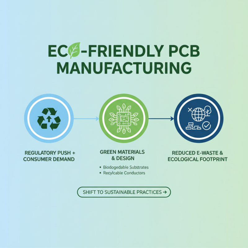
Environmental Regulations: Adapting PCB Designs for Eco-Friendly Manufacturing
As electronic circuits become increasingly integral to modern technology, environmental regulations are pushing PCB designers to rethink their approaches to manufacturing. The shift towards eco-friendly production methods is not merely a trend but a necessity driven by both consumer demand and regulatory pressure. Designers are now exploring materials that comply with stricter environmental standards, emphasizing the use of biodegradable and recyclable substances in PCB manufacturing. This transition is paving the way for sustainable practices, ultimately reducing the ecological footprint associated with electronic waste.
In adapting to these regulations, PCB designers are incorporating innovative techniques that maximize material efficiency and minimize toxic emissions. Advanced manufacturing processes, such as additive printing and laser cutting, are gaining traction as they allow for greater precision and less material waste. Additionally, the use of lead-free solder and non-toxic coatings aligns with emerging guidelines, ensuring compliance while maintaining the performance and longevity of the circuits. As these eco-friendly practices become standard, designers are challenged to balance functionality and sustainability, fostering a new era of environmentally responsible electronics.