In the rapidly evolving field of electronics, mastering the art of PCB fabrication is essential for both beginners and seasoned professionals. As advancements in technology continue to drive the demand for more sophisticated printed circuit boards, understanding the fundamental principles behind PCB fabrication becomes crucial. "The key to effective PCB fabrication lies not only in the technical skills but also in the attention to detail and understanding of the materials," says Dr. Emily Carter, a renowned expert in the PCB industry. Her insights highlight the importance of both knowledge and precision in producing high-quality boards.
Whether you are designing for a simple hobby project or a complex commercial application, the intricacies of PCB fabrication can be daunting. This guide aims to provide a comprehensive overview of the top ten tips that cater to individuals at any level of expertise. From layout considerations to selecting the right materials, each tip is designed to enhance your understanding and execution of PCB fabrication. By following these guidelines, you will not only improve the reliability and performance of your circuits but also gain confidence in your ability to navigate the challenges of this critical manufacturing process.
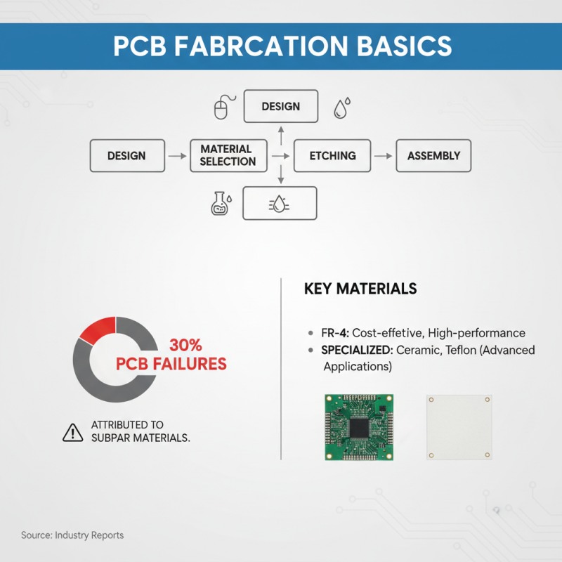
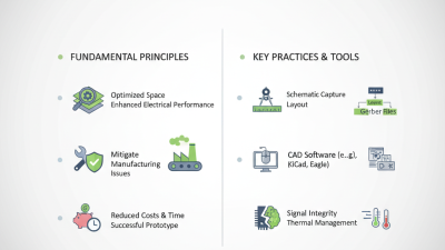
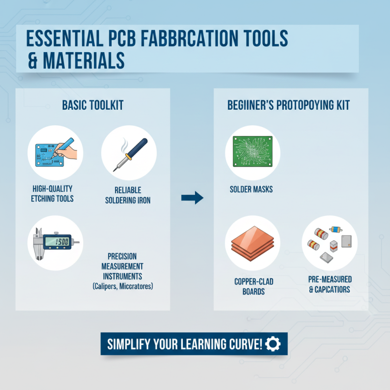
Understanding the basics of PCB fabrication is essential for both beginners and seasoned professionals. The PCB manufacturing process generally involves steps like design, material selection, etching, and assembly. A critical aspect of this process is the use of high-quality materials. According to industry reports, nearly 30% of PCB failures can be attributed to subpar materials, highlighting the importance of choosing the right substrate and components. For instance, FR-4 remains the most widely used material for PCB fabrication due to its excellent balance of cost and performance, but advanced applications may require specialized materials such as ceramic or Teflon laminates.
Furthermore, beginners should pay attention to design for manufacturability (DFM) to reduce potential pitfalls during production. Studies suggest that up to 70% of manufacturing issues arise from design flaws, making it crucial to adhere to best practices in PCB layout. Techniques like maintaining adequate trace width and spacing can enhance reliability and performance. Additionally, leveraging CAD tools effectively can streamline the design process, allowing for iterations and improvements before moving to fabrication. Understanding these fundamental concepts not only prepares newcomers for successful PCB projects but also empowers professionals to optimize their workflows and improve product reliability.
When diving into PCB fabrication, having the right tools and materials can significantly impact the quality of your work. A basic toolkit should include high-quality etching tools, a reliable soldering iron, and precision measurement instruments such as calipers and micrometers. For beginners, starting with a PCB prototyping kit can be incredibly beneficial, as it often contains essential components like solder masks, copper-clad boards, and pre-measured resistors and capacitors. Such kits simplify the learning curve and allow users to focus on understanding the fabrication process without becoming overwhelmed.
In addition to tools, the choice of materials plays a crucial role in ensuring successful PCB fabrication. The substrate, typically made from fiberglass or phenolic, must be carefully chosen based on the project's requirements. Copper foil, which serves as the conductive layer, should also be of good quality and appropriate thickness to withstand the soldering process. Other materials like photoresists, cleaning solvents, and protective coatings are essential for achieving excellent results. A well-curated selection of these materials will not only enhance the fabrication process but also contribute to the longevity and reliability of the final product.
Designing a PCB layout effectively requires a clear understanding of the project requirements and the electronic components involved. Start by creating a schematic diagram that outlines the interconnections between components. This step is vital as it serves as the blueprint for your layout. Ensure to include all necessary elements such as resistors, capacitors, and ICs, while also considering the signal flow to maintain functionality. A meticulously crafted schematic not only simplifies the layout process but also minimizes errors during the fabrication phase.
Once your schematic is finalized, you can move on to the actual layout. Begin by placing the components on the board, keeping in mind their physical dimensions and pin configurations. Aim for a tidy arrangement that reduces trace lengths and avoids crossing lines whenever possible. Use ground planes generously to enhance performance and minimize electromagnetic interference. Pay close attention to the rules set by your PCB fabrication house regarding trace width, spacing, and maximum layer counts to ensure manufacturability. Finally, utilize design rule checks (DRC) to catch any potential errors before finalizing your design. This systematic approach will help you create a robust and effective PCB layout tailored to your project’s needs.
When it comes to PCB fabrication, common mistakes can significantly affect the final product, leading to increased costs and project delays. According to a report by IPC, nearly 50% of all PCB failures can be attributed to design errors made during the initial stages of development. One of the primary pitfalls beginners and professionals alike encounter is neglecting the importance of thorough design validation. Before moving forward with fabrication, conducting comprehensive design rule checks (DRC) can significantly reduce errors and ensure a smoother prototyping process.
Another frequent mistake relates to the choice of materials. A lack of understanding of materials specifications often leads to selecting inappropriate substrates, which can compromise the PCB’s performance. Research from the Electronic Industries Alliance indicates that over 20% of PCB fabrication issues stem from material selection errors. To mitigate this risk, always refer to material datasheets and verify that your selections align with the operational environment of your final product.
Lastly, assembling PCBs without proper communication between engineering and manufacturing teams can create discrepancies that lead to costly reworks. Implementing a collaborative approach helps to align design specifications with manufacturing capabilities from the outset. Effective communication channels can foster better understanding and ensure that both teams are on the same page, reducing the potential for errors during assembly.
Quality control is an essential step in the PCB fabrication process. Proper testing and troubleshooting methods can significantly reduce the likelihood of failures and improve the overall reliability of electronic devices. According to industry data from IPC, nearly 60% of PCB failures stem from design errors and manufacturing flaws. Therefore, implementing stringent quality control measures is not only beneficial but also crucial for maintaining high standards in PCB production.
One effective tip for beginners is to utilize Design Rule Checks (DRC) during the PCB design phase. DRC software tools identify potential design issues before fabrication, reducing the chances of defects. Additionally, performing electrical tests on the finished PCB can reveal any short circuits or open circuits, ensuring that the final product meets the required specifications.
For professionals, adopting advanced testing techniques, such as Automated Optical Inspection (AOI) and X-ray inspection, can further enhance quality control. These methods provide detailed analysis and real-time feedback, helping to pinpoint defects in complex multi-layer boards. Implementing such thorough testing protocols aligns with findings that illustrate a 30% improvement in defect detection rates, ultimately leading to reduced rework and a more reliable end product.
| Cookie | Duration | Description |
|---|---|---|
| cookielawinfo-checkbox-analytics | 11 months | This cookie is set by GDPR Cookie Consent plugin. The cookie is used to store the user consent for the cookies in the category "Analytics". |
| cookielawinfo-checkbox-functional | 11 months | The cookie is set by GDPR cookie consent to record the user consent for the cookies in the category "Functional". |
| cookielawinfo-checkbox-necessary | 11 months | This cookie is set by GDPR Cookie Consent plugin. The cookies is used to store the user consent for the cookies in the category "Necessary". |
| cookielawinfo-checkbox-others | 11 months | This cookie is set by GDPR Cookie Consent plugin. The cookie is used to store the user consent for the cookies in the category "Other. |
| cookielawinfo-checkbox-performance | 11 months | This cookie is set by GDPR Cookie Consent plugin. The cookie is used to store the user consent for the cookies in the category "Performance". |
| viewed_cookie_policy | 11 months | The cookie is set by the GDPR Cookie Consent plugin and is used to store whether or not user has consented to the use of cookies. It does not store any personal data. |