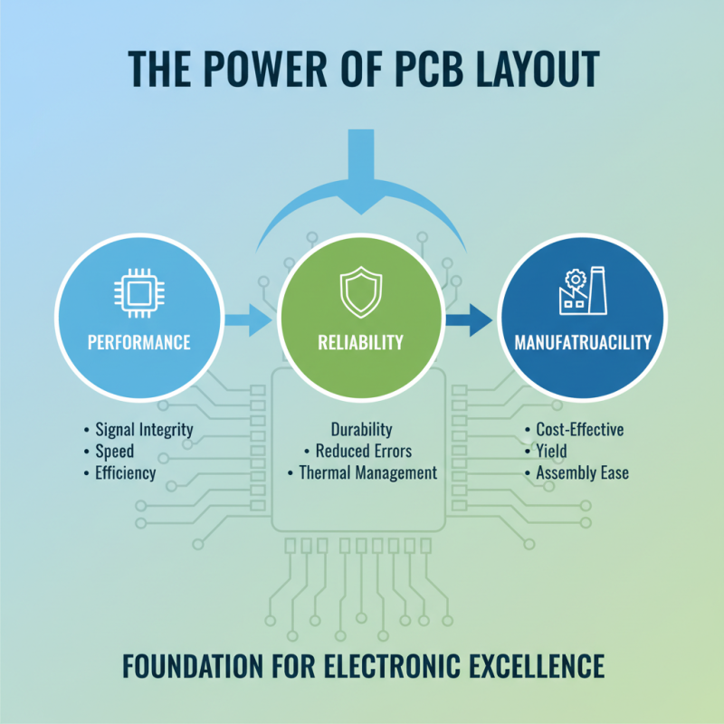
In the realm of electronics design, the significance of PCB layout cannot be overstated. As the foundation upon which electronic circuits are built, a well-crafted PCB layout directly influences the performance, reliability, and manufacturability of electronic devices. Renowned expert in the field, Dr. Emily Tran, emphasizes this importance by stating, “A meticulously designed PCB layout not only enhances the efficiency of electronic systems but also minimizes costly errors during production.”
The art and science of PCB layout involve numerous considerations, from component placement to trace routing, that can dramatically affect the electrical characteristics of the final product. Poor layout decisions can lead to signal integrity issues, increased electromagnetic interference, and thermal management problems, potentially jeopardizing the success of the entire project. Therefore, understanding the principles of effective PCB layout is crucial for engineers and designers aiming to create high-quality electronic products that meet market demands.
As technology continues to evolve, the complexity of devices increases, making it even more vital for designers to acquire a strong grasp of PCB layout principles. By focusing on optimal design strategies, engineers can ensure that their electronic products not only function as intended but also excel in a competitive landscape, ultimately fostering innovation and advancement in the electronics industry.


The significance of PCB layout in electronics design cannot be overstated, as it serves as the foundation for the performance, reliability, and manufacturability of electronic devices. A well-executed PCB layout ensures that components are placed strategically and that signal integrity is maintained, which is crucial for avoiding issues like cross-talk and electromagnetic interference. When designing a PCB, engineers must consider the physical arrangement of components, trace routing, and the overall flow of electrical signals to optimize the function of the entire system.
**Tips:** When laying out your PCB, always prioritize the placement of high-frequency components and sensitive analog parts to minimize noise and interference. Additionally, ensure that ground planes are utilized effectively to provide a stable reference for voltage levels and improve signal quality.
Another important aspect of PCB layout is thermal management. With electronic devices generating heat, the layout must allow for proper heat dissipation to prevent component overheating, which can lead to failure. Engineers should carefully design the positioning of heat-sensitive components and incorporate thermal vias or heat sinks as necessary to secure longevity and efficiency in device operation.
**Tips:** Consider using thermal simulation tools during the design phase to predict and evaluate how heat will flow through your PCB. This proactive approach can help you make necessary adjustments early on, ensuring the reliability of your final product.
Effective PCB layout techniques are pivotal in the electronics design process, significantly influencing the performance, reliability, and manufacturability of electronic devices. A well-structured PCB layout minimizes electromagnetic interference (EMI) and crosstalk, which can drastically affect signal integrity. According to a report by IPC, approximately 60% of all PCB-related failures are attributed to poor layout designs. This statistic underscores the necessity for careful planning and execution during the design phase to ensure optimal functionality.
One of the key principles of effective PCB layout is the strategic placement of components. By grouping related components and following signal path optimization guidelines, designers can reduce the length of trace connections, thereby minimizing resistance and enhancing performance. Additionally, maintaining appropriate spacing between high-frequency signal lines can mitigate interference, ensuring that the board operates effectively at its intended frequencies. Reports indicate that careful component placement coupled with a thorough understanding of grounding techniques can lead to design efficiency improvements of up to 30%, which is crucial in today’s fast-paced electronics market where performance and reliability are paramount.
The layout of a printed circuit board (PCB) plays a pivotal role in the overall performance and reliability of electronic devices. A well-optimized PCB layout minimizes unwanted effects such as signal degradation and electromagnetic interference (EMI). According to a report from IPC, the association connecting electronics industries, improper PCB design accounts for approximately 25% of product failures in the electronics sector. This underscores the necessity of meticulous design practices, especially when it comes to maintaining signal integrity.
Signal integrity is fundamentally influenced by the PCB layout, impacting factors such as trace width, spacing, and the use of ground planes. Research from the IEEE has shown that signal loss can increase by up to 20% due to poor routing techniques and inadequate spacing between traces. The presence of return paths, controlled impedance design, and minimizing loop areas are critical aspects that can help mitigate these issues. Similarly, a study published in the Journal of Electronic Materials indicated that designs with optimized layouts could achieve a threefold improvement in performance stability, especially in high-speed applications where signal integrity is paramount. These statistics not only highlight the significance of effective PCB design but also suggest a direct correlation between layout strategies and the performance longevity of electronic products.
PCB layout plays a pivotal role in the overall success of electronic design, but it is not without its challenges. According to a recent industry report by IPC, improper layout can account for over 50% of failures in electronic devices during testing and post-manufacturing phases. Common challenges such as signal integrity, thermal management, and component placement need to be meticulously addressed to ensure optimal performance. For instance, high-speed designs often face significant issues related to electromagnetic interference (EMI) and crosstalk, which can be mitigated through careful routing and the use of ground planes.
To overcome these hurdles, designers can adopt best practices such as utilizing design rule checks (DRC) and simulations early in the design process. These tools can help identify potential issues before production, leading to substantial cost savings and improved reliability. Research from the Institute of Electrical and Electronics Engineers (IEEE) indicates that employing simulation tools can reduce the time spent on PCB iterations by up to 30%, allowing engineers to focus on refining their designs instead of fixing problems post-production. Emphasizing a robust approach to PCB layout not only enhances device functionality but also contributes to the longevity and efficiency of electronic products in a rapidly evolving market.
When designing a printed circuit board (PCB), achieving an optimal layout is essential for successful electronics manufacturing. One of the best practices is to maintain a proper grounding strategy. A solid ground plane not only helps in reducing electromagnetic interference but also improves the performance of high-speed signals. By minimizing the distance between the components and the ground plane, designers can achieve better signal integrity, which is critical for modern electronic devices.
Another vital aspect is to consider the component placement and routing carefully. It is crucial to position components based on their function, avoiding long traces that can introduce resistance and capacitance, which may affect the signal. Placing decoupling capacitors close to power pins can stabilize the voltage and mitigate noise. Additionally, adhering to a consistent trace width and using appropriate vias can enhance manufacturability and reliability of the PCB. Following these techniques can significantly streamline the production process, reduce assembly errors, and improve the overall performance of the electronic design.
| Design Aspect | Best Practices | Impact on Manufacturing | Common Pitfalls |
|---|---|---|---|
| Component Placement | Optimize for signal flow and thermal management. | Reduces assembly time and improves performance. | Crowded layouts can lead to errors. |
| Trace Width | Calculate trace widths based on current carrying capacity. | Prevents overheating and signal integrity issues. | Using too narrow traces can cause failures. |
| Layer Stackup | Use appropriate layer configurations for RF and high-speed designs. | Enhances signal integrity and reduces EMI. | Inadequate stackup can lead to performance issues. |
| Ground Planes | Include solid ground planes to minimize noise. | Improves overall circuit performance. | Skipping ground planes can increase circuit noise. |
| DRC Checks | Regularly perform Design Rule Checks throughout the layout process. | Identifies potential issues early, saving time and cost. | Ignoring DRC can lead to costly reworks. |


| Cookie | Duration | Description |
|---|---|---|
| cookielawinfo-checkbox-analytics | 11 months | This cookie is set by GDPR Cookie Consent plugin. The cookie is used to store the user consent for the cookies in the category "Analytics". |
| cookielawinfo-checkbox-functional | 11 months | The cookie is set by GDPR cookie consent to record the user consent for the cookies in the category "Functional". |
| cookielawinfo-checkbox-necessary | 11 months | This cookie is set by GDPR Cookie Consent plugin. The cookies is used to store the user consent for the cookies in the category "Necessary". |
| cookielawinfo-checkbox-others | 11 months | This cookie is set by GDPR Cookie Consent plugin. The cookie is used to store the user consent for the cookies in the category "Other. |
| cookielawinfo-checkbox-performance | 11 months | This cookie is set by GDPR Cookie Consent plugin. The cookie is used to store the user consent for the cookies in the category "Performance". |
| viewed_cookie_policy | 11 months | The cookie is set by the GDPR Cookie Consent plugin and is used to store whether or not user has consented to the use of cookies. It does not store any personal data. |