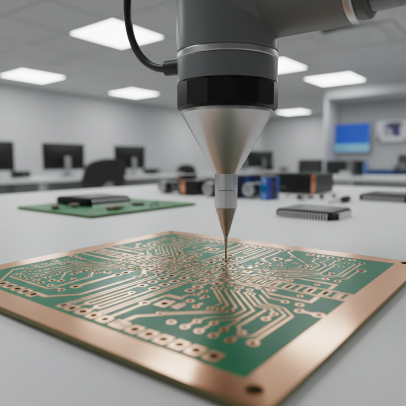
What is PCB Printing and How Does It Work?
PCB printing is a crucial process in modern electronics. It creates printed circuit boards that are the backbone of electronic devices. Understanding how PCB printing works is vital for engineers and hobbyists alike.
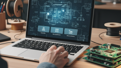
The process begins with a design. A schematic is converted into a layout. This layout guides the placement of components on the board. The accuracy of this stage influences the final product. Many overlook this step, leading to malfunctions later.
Once the design is set, materials are prepared. Copper layers are laminated onto a substrate. This is where things can get tricky. Any imperfections can cause short circuits. This highlights the importance of precision in PCB printing. As technology advances, new printing methods emerge. Keeping up with these changes is important for staying competitive.
What is PCB Printing? An Overview of the Process
PCB printing, or printed circuit board printing, is a crucial process in modern electronics. It transforms digital designs into physical circuits. The process begins with designing a layout using computer-aided design (CAD) software. This software helps engineers visualize electrical connections and components. According to a recent industry report, the global PCB market is expected to reach over $80 billion by 2026, driven by the increasing demand for consumer electronics.
Once the design is finalized, printing begins. The boards are made from materials like FR-4, a flame-retardant glass-epoxy composite. The printed circuit patterns are created using various techniques, including screen printing and photolithography. In screen printing, conductive inks are applied directly onto the substrate. Photolithography involves coating the board with a light-sensitive material, exposing it to UV light, and developing it to reveal the circuit pattern. This method ensures precise replication of complex designs. However, it often requires fine-tuning and can lead to production inconsistencies.
Post-printing, the boards undergo cleaning and inspection processes. These steps are vital for quality assurance. Any defects, like shorts or opens, can lead to malfunctioning devices. Despite the advanced technology available, challenges remain in maintaining consistent quality across different batches. The industry continues to seek improvements, as even minor errors can have significant impacts on overall performance and reliability.
The Essential Components of PCB Printing
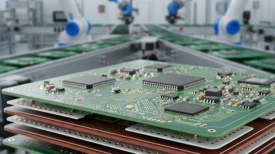
PCB printing, also known as printed circuit board fabrication, involves several essential components that are critical to the process. The core elements include the substrate, conductive pathways, and solder mask. The substrate is typically made of fiberglass or epoxy resin, providing the necessary structural support. Conductive pathways, often created using copper, facilitate the electrical connections between components. The solder mask, applied over the copper traces, protects the circuitry and helps prevent short circuits.
Industry reports indicate that the global PCB market is projected to reach $73 billion by 2026, driven by innovations in technology and increased demand for electronics. This growth highlights the importance of optimizing PCB printing processes. Factors like layer count, trace width, and spacing must be carefully managed. Precision is key; small errors can lead to significant failures in electronic devices.
Tip: Always double-check your designs before printing. Errors in spacing and width can lead to production delays. Additionally, consider using software designed for PCB layout to minimize mistakes. Keep in mind, not all designs will turn out perfectly, so be prepared to iterate on your prototypes. Learning from each print can lead to better results over time. Another point to reflect on: balance quality with cost. Sometimes, cheaper materials can compromise the integrity of the final product, impacting durability and performance.
Step-by-Step Guide to the PCB Printing Process
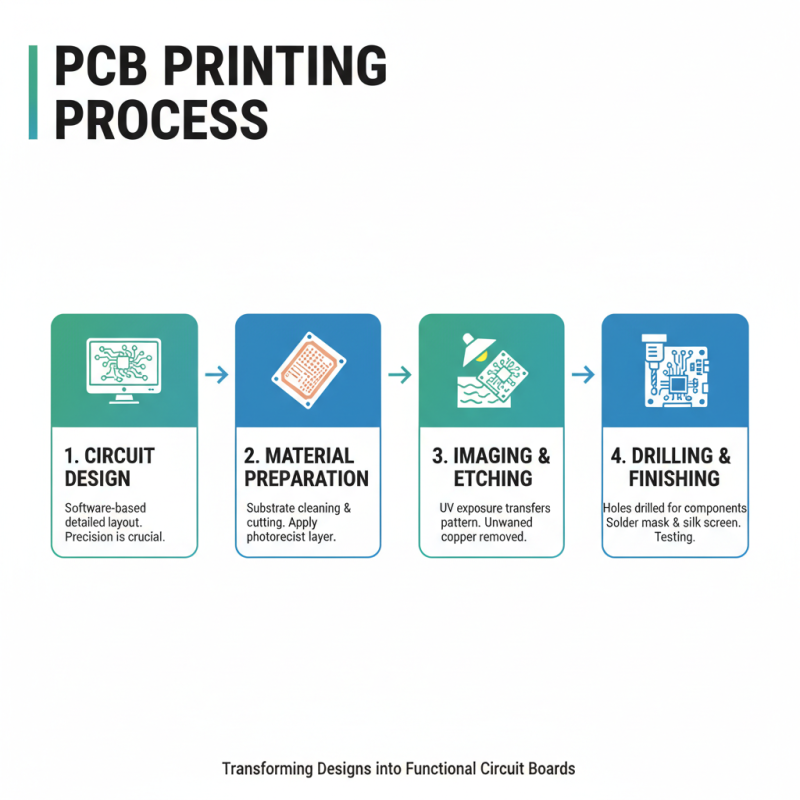
PCB printing is a complex process that transforms designs into functional circuit boards. It begins with a detailed layout of the circuit. This design is usually created using specialized software and must be precise. Any mistakes here can lead to failures later.
After finalizing the design, it’s time to print the layers. Each layer is crucial and must align perfectly. Photosensitive materials are commonly used. Light exposes these materials to create the circuit patterns. This stage requires careful calibration. A slight error can lead to significant problems.
Tips: Always double-check the design files. Look for any inconsistencies or mistakes. It’s easy to overlook small details.
Once the layers are printed, they’re etched to remove excess material. This is where the actual circuits take shape. After etching, the boards are drilled for components. The holes must be accurate. Inaccuracies can complicate assembly.
Tips: Clean the board after etching. Residue can affect performance. A clean workspace also helps you focus better.
Next, all components are soldered onto the board. This step requires patience and precision. Poor soldering can lead to short circuits. A steady hand is essential, and a magnifying glass can be helpful.
Assembling PCBs is an art as much as a science. Embrace the challenges, learn from mistakes, and continuously refine your process.
Types of PCB Printing Techniques Used Today
PCB printing is an essential process in the electronics manufacturing industry. It involves different techniques to create circuit boards effectively. Among the many methods, two stand out: screen printing and digital printing. Each technique has its unique advantages and challenges.
Screen printing is a traditional method that uses a stencil to apply conductive ink onto the PCB. It allows for precise and high-quality designs. However, it can be time-consuming. The setup requires careful measurements. Mistakes in alignment can lead to defects. Digital printing, on the other hand, is faster and more flexible. It directly prints designs onto the surface. This method supports quick changes, but it may not yield the same durability as screen printing.
Another technique gaining attention is inkjet printing. This method uses tiny droplets of ink to create intricate designs. While it offers high resolution, it can struggle with thicker materials. Each printing method has its strengths and weaknesses. Selecting the right one depends on the specific project requirements. Practitioners must weigh these factors carefully. Adjustments may be necessary. Achieving the perfect PCB still requires ongoing refinement.
Applications and Significance of PCB Printing in Electronics
PCB printing plays a crucial role in modern electronics. The applications of printed circuit boards (PCBs) are vast, ranging from consumer electronic devices to advanced medical equipment. According to a recent market report, the global PCB market was valued at over $60 billion in 2022 and is projected to grow significantly over the next few years. This growth reflects the increasing demand for electronic gadgets and the effectiveness of PCB technology in various sectors.
In consumer electronics, PCBs allow compact and efficient designs. They enable smartphones to pack more features without increasing size. Moreover, in the automotive industry, PCBs are vital for safety systems and navigation controls. They support advanced driver-assistance systems (ADAS), improving vehicle safety. The significance of PCBs also extends to renewable energy, where they are essential in solar panels and wind turbines.
Tip: Regular maintenance of PCB-equipped devices is essential. Overheating can cause failures. Clean connections regularly to ensure optimal performance.
Despite these advantages, PCB manufacturing poses some challenges. The process can be wasteful, with many materials not fully utilized. There are also environmental impacts associated with the production. As technology evolves, the industry must address these issues. Sustainable practices can enhance the PCB manufacturing process while meeting growing demands. It's a balancing act that requires innovation and responsibility.
| Aspect |
Description |
Applications |
Significance |
| Definition |
PCB printing refers to the process of creating printed circuit boards (PCBs) which are used to connect electronic components. |
Consumer electronics, medical devices, automotive electronics, industrial machinery. |
Essential for functionality, reliability, and compactness of electronic devices. |
| Methods |
Common methods include silkscreen printing, inkjet printing, and laser etching. |
Rapid prototyping, low-volume production, and custom designs. |
Allows for quick turnaround times and customization in design. |
| Materials |
Common materials include FR-4, CEM1, and flexible substrates. |
Used in various sectors like telecommunications and aerospace. |
Material choice affects durability, heat resistance, and performance of the PCB. |
| Challenges |
Challenges include design complexity, manufacturing precision, and quality assurance. |
High-tech applications like smartphones and laptops where reliability is critical. |
Ensures safety and efficiency in high-stakes electronic applications. |