How to Start PCB Printing for Your Electronics Projects?
PCB printing is an evolving field that offers new possibilities for electronics enthusiasts. According to Dr. Jenna Hayes, an expert in the PCB printing industry, "The right process can empower anyone to create robust electronic designs." With the right tools and knowledge, anyone can turn ideas into tangible products.
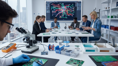
Getting started with PCB printing may seem daunting. Beginners often feel overwhelmed by design software, material choices, and machinery. Mistakes are common, like miscalculating measurements or using inappropriate substrates. However, these missteps offer vital learning opportunities. Adapting to challenges helps build better projects.
As you dive deeper into PCB printing, embrace experimentation. The learning curve might seem steep, but persistence pays off. Each project reflects your growth and creativity. Make use of online forums and communities for support and inspiration. The journey of PCB printing is as valuable as the end result.
Understanding the Basics of PCB Printing for Electronics Projects
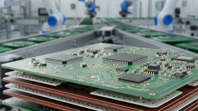
Printing PCB for electronics projects can seem challenging. However, understanding the basics will simplify the process. A printed circuit board (PCB) connects various components in electronic devices. In recent years, the global PCB market has grown significantly, reaching approximately $70 billion in 2022. This growth showcases the rising demand for electronic devices.
When starting your PCB printing, consider different methods. Traditional methods include etching and milling. Both have pros and cons. For example, etching can produce high-quality boards but may involve complex chemical handling. On the other hand, milling is safer and more straightforward but may lack precision.
Tips: Always use high-quality materials. Low-grade substrates can impact performance. Also, be aware of potential issues like design errors and component placement mistakes. These faults can lead to costly revisions. Remember, learning from failures is vital. Each misstep provides valuable insights into your process. Exploring online forums and communities can also lead to newfound knowledge.
Choosing the Right PCB Printing Method for Your Needs
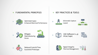
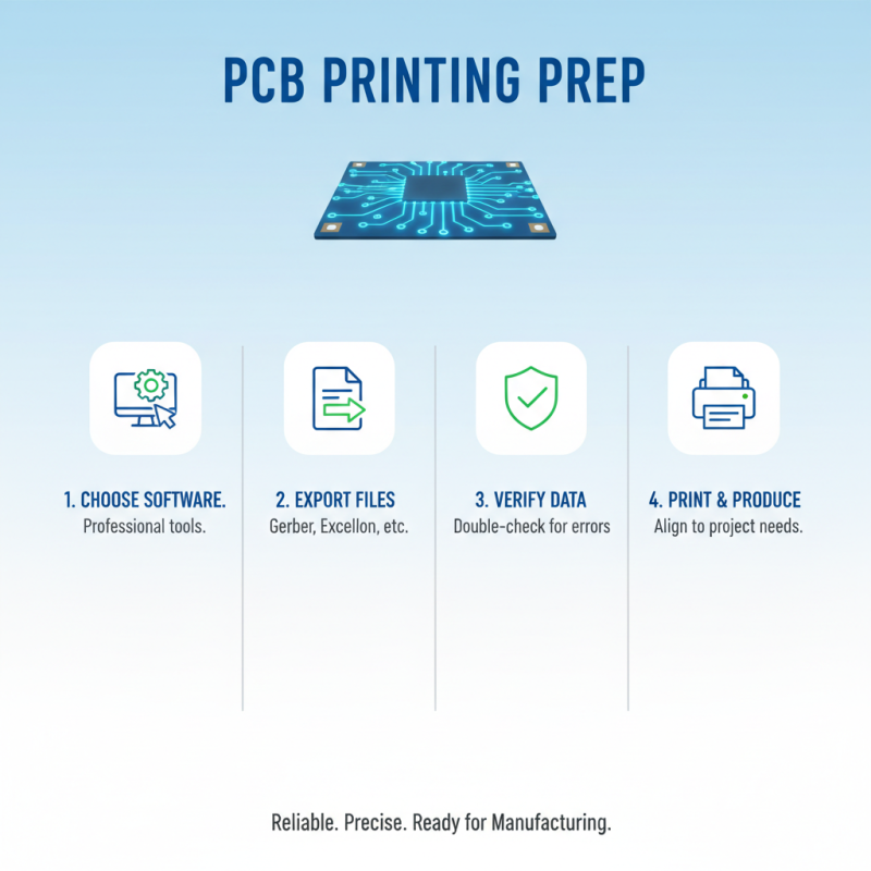
Choosing the right PCB printing method is crucial for your electronics projects. Each method has its pros and cons. The most common methods include inkjet printing, laser printing, and photo-etching. Inkjet printing is affordable and user-friendly. However, it may not provide the durability needed for complex circuits. If you choose laser printing, you can get higher precision. Yet, you might need specialized film and a good printer.
Photo-etching is excellent for intricate designs. It creates clean lines and detailed features. But this method can be time-consuming and requires additional chemicals. Make sure you have the right setup before diving into this. You might run into issues with alignment or exposure time. Testing each method on a small scale is wise. This way, you can avoid costly mistakes later. Evaluate your needs and budget before settling on a method. Each project may call for a different approach. Explore them thoroughly; your success depends on it.
PCB Printing Methods and Their Popularity
Selecting Materials and Components for Your PCB
When starting PCB printing for electronics projects, selecting the right materials and components is crucial. The base material, typically FR4, varies in quality. A report by IPC shows that improper material can lead to a significant 25% increase in failure rates. Choosing the appropriate copper thickness affects conductivity. Thicker copper can support higher currents but adds cost.
Tips: Always check material specifications. Look for suppliers who provide detailed data sheets. This helps ensure compatibility and performance.
Components are just as vital. Resistors, capacitors, and traces must be chosen based on the circuit's requirements. For example, choosing low-ESR capacitors can reduce losses. However, they can be harder to source. Balancing quality and cost is a common dilemma.
Tips: Prototype with cheaper materials first. This approach allows for design iteration without heavy investment. Reflect on failures; they often provide the best learning experiences. Consider potential issues early on. Revisit your choices if problems arise.
Post-Printing Steps: Testing and Assembling Your PCB
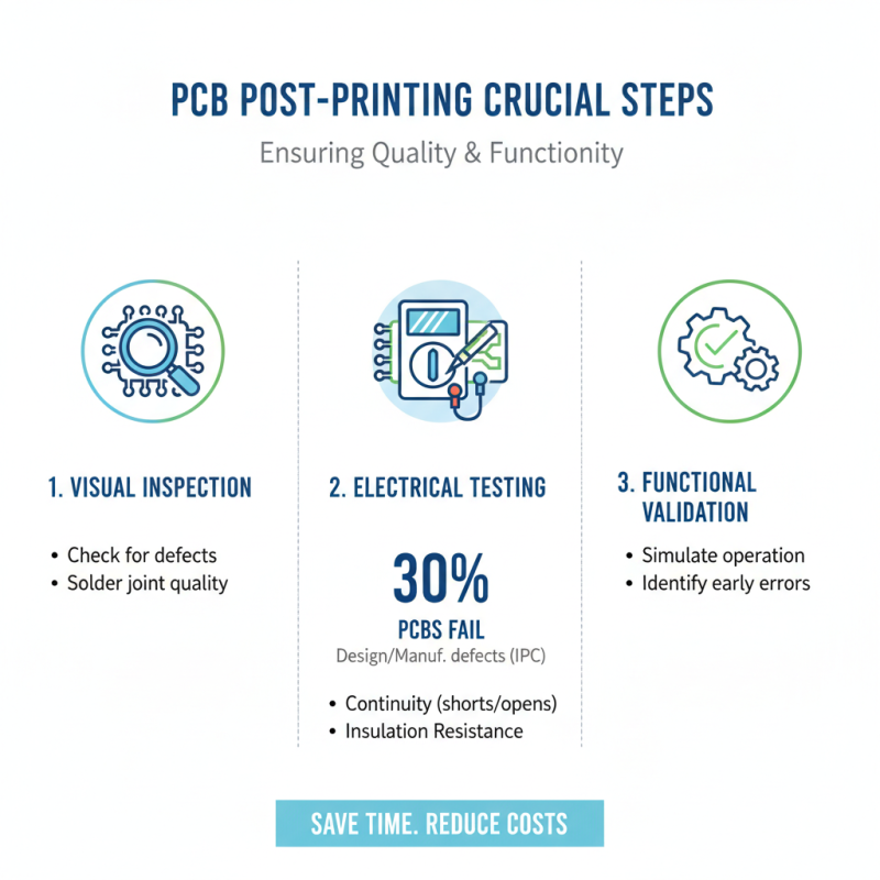
After printing your PCB, several important steps follow. Testing is crucial to ensure functionality. A report by IPC states that over 30% of PCBs fail during testing due to design issues or manufacturing defects. Common tests include electrical continuity and insulation resistance. These tests can highlight potential errors early, saving time and cost later.
Assembling your PCB involves meticulous attention to detail. Start with component placement, ensuring each part aligns with the design. Soldering is the next step, but it requires skill and practice. Many hobbyists struggle with soldering, resulting in cold joints or short circuits. Regularly reviewing your methods can help identify areas for improvement.
After assembly, again test your PCB’s functionality. Many overlook this step, leading to frustration during the project. Using tools such as multimeters can help confirm that each connection is working as intended. Understanding these post-printing steps is key to successful electronics projects.