What Is a Flexible PCB and How Does It Work?

What Is a Flexible PCB and How Does It Work?

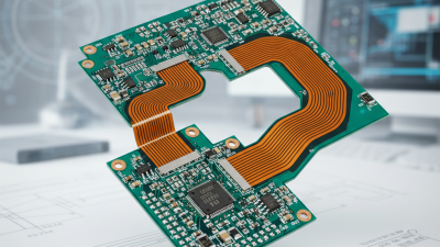
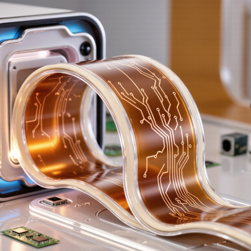
A flexible pcb is a thin circuit board designed to bend, fold, or move inside electronic products. Unlike rigid FR-4 boards, it uses polymer films, often polyimide, as its base material. Copper traces are laminated onto this film and protected with flexible cover layers. These layers work together like a narrow electrical ribbon.

When current travels through the copper paths, the circuit performs the same basic function as a rigid board. The difference appears in its mechanical behavior. A flexible pcb can follow a camera hinge, wrap around a medical sensor, or fit inside a compact wireless device. That movement reduces connectors and saves valuable space. It can also lower assembly weight.

The phrase “flexible” can mislead. It does not mean unlimited bending. Engineers must control bend radius, copper thickness, layer arrangement, and strain relief. Repeated folding can damage traces, especially near sharp corners or unsupported transitions. In practical design work, these details often decide whether a prototype survives production testing.

Manufacturers commonly follow IPC-2223 guidance for flexible and flex-rigid circuit design. They also inspect impedance, insulation, solder joints, and dimensional stability. Real-world reliability depends on material selection and manufacturing control, not appearance alone. A slim board may still fail.

This article explains how flexible pcb structures are built and how electrical signals move through them. It also examines their benefits, limitations, common applications, and the design choices that influence service life. Some trade-offs remain unavoidable. That is where careful engineering matters.
What Is a Flexible PCB and How Does It Work?

What Is a Flexible PCB and What Makes It Different?

A flexible PCB is a circuit board built on a bendable polymer film. Unlike a rigid PCB, it can fold, twist, or fit around tight spaces. Rigid boards depend on fiberglass layers for structural support. Flexible boards commonly use polyimide, copper foil, and adhesive films. These materials allow electrical paths to move with the product. The difference is mechanical as much as electrical.

The 2024 Research and Markets outlook projects the flexible PCB market to grow at roughly 11% annually through 2030. This growth reflects smaller devices, wearable products, and compact automotive systems.

Yet flexibility does not mean unlimited movement. Repeated bending creates copper fatigue, especially near sharp corners. IPC-2223 design guidance recommends controlled bend radii and careful layer construction. A careless radius can damage hidden traces.

During assembly, engineers often leave extra length near connectors. This reduces stress when the circuit moves during installation.

Dynamic flexing needs different testing from a one-time fold. Static bending may work in a prototype, then fail after thousands of cycles. That trade-off is easy to underestimate. Thermal expansion also changes the design, because copper and polymer materials expand differently. Engineers should review routing, insulation, and bend zones together, not separately.


What Materials and Layers Form a Flexible PCB?

A flexible PCB usually begins with a polyimide film, often 25–125 micrometers thick. Polyimide tolerates heat and repeated bending better than many plastic films. Liquid-crystal polymer is another option for high-frequency circuits, although its processing window can be less forgiving. A 2024 flexible electronics market analysis projected double-digit annual growth through 2030, reflecting demand for thinner wearable and automotive assemblies.

Copper forms the conductive layer. Rolled-annealed copper bends more reliably than standard electrodeposited copper, especially in dynamic applications. Typical copper thickness ranges from 12 to 35 micrometers. The circuit may use one, two, or several copper layers. Polyimide coverlay protects exposed traces, while adhesive bonds the coverlay to copper. Adhesiveless constructions reduce thickness and improve thermal stability. They also cost more.

The layer stack is never perfectly simple. Surface finishes protect contact pads from oxidation. Stiffeners support connectors and component areas, but they reduce local flexibility. IPC-2223C recommends designing bend zones around actual material behavior, not only nominal thickness. A common engineering rule uses a bend radius of at least six times the finished thickness for static bending. Dynamic flexing often needs a larger radius. Laboratory results can look excellent. Production handling may still expose weak vias, sharp corners, or uneven adhesive flow. That gap deserves careful review.

What Is a Flexible PCB and How Does It Work? — Materials and Layers

Layer or Parameter Typical Material Typical Thickness Primary Function Key Performance Characteristics
Base Film Polyimide film 12.5–50 μm Provides the flexible mechanical foundation and electrically insulates the copper circuit. High thermal stability, good dimensional stability, low moisture absorption, and resistance to repeated flexing.
Conductor Layer Rolled-annealed copper or electrodeposited copper 18–70 μm Carries electrical current and forms signal, power, and ground traces. Rolled-annealed copper is generally preferred for dynamic bending because it offers good ductility and fatigue resistance.
Coverlay Polyimide film with flexible adhesive 25–75 μm Covers and protects exposed copper traces while providing electrical insulation. Improves abrasion resistance and environmental protection; openings are formed over pads and contact areas.
Flexible Adhesive Acrylic or epoxy adhesive 15–50 μm Attaches the copper foil to the base film or bonds the coverlay to the circuit. Must retain adhesion during thermal cycling and flexing; adhesive thickness affects total board thickness and bend performance.
Stiffener Polyimide, polyester, or glass-reinforced epoxy laminate 50–300 μm Locally reinforces connector fingers, component areas, and assembly zones. Provides insertion strength and dimensional support without making the entire circuit rigid.
Surface Finish Electroless nickel immersion gold, immersion tin, or organic solderability preservative Process-dependent Protects exposed copper pads and supports soldering or electrical contact. Selection depends on contact durability, soldering requirements, storage life, and cost considerations.
Single-Sided Construction One copper layer between a base film and protective coverlay Commonly 0.10–0.30 mm overall Supports simple interconnects with a single conductive layer. Lowest complexity and high flexibility; suitable when routing does not need crossovers or multiple signal layers.
Double-Sided Construction Two copper layers separated by a flexible dielectric layer Commonly 0.20–0.50 mm overall Allows routing on both sides of the dielectric and electrical connection through plated vias. Provides greater routing density while remaining flexible; bend zones should avoid unnecessary vias and stiff features.
Multilayer Construction Multiple copper and flexible dielectric layers bonded together Commonly 0.30–0.80 mm overall Combines several routing, power, and ground layers in a compact flexible assembly. Higher density and better signal-integrity options, but lower flexibility and greater manufacturing complexity than simpler constructions.
Dynamic Bend Radius Determined by material stack-up and copper design Often at least 10× the total thickness Defines the minimum radius for repeated flexing during normal operation. Dynamic applications generally require a larger radius than one-time folding; fewer layers and thinner copper improve flex life.
Static Bend Radius Determined by material stack-up and bend direction Often at least 6× the total thickness Defines the minimum radius when the flexible circuit is formed once and remains in position. Actual limits depend on copper type, trace geometry, bend angle, temperature, and the number of forming cycles.
Electrical Operating Principle Conductive copper traces separated by dielectric films Not applicable Transmits power and electrical signals between components, connectors, and rigid circuit boards. Flexibility comes from the thin polymer-based stack-up, while circuit behavior follows the same basic electrical principles as a rigid PCB.
Typical values are design ranges rather than universal limits. Final thickness, bend radius, and material selection depend on the circuit layout, operating temperature, flexing cycles, and manufacturing requirements.

How Does a Flexible PCB Carry Electrical Signals?

A flexible PCB carries electrical signals through thin copper traces laminated between polymer films. The copper acts like miniature wiring, while the dielectric layers separate conductors and control signal behavior. At a connector, exposed copper pads transfer current to another circuit. Along the route, electrons respond to voltage differences, not to the board’s shape.

Signal quality depends on trace width, copper thickness, spacing, and dielectric thickness. These dimensions influence resistance, capacitance, and impedance. A narrow trace has higher resistance and can produce greater voltage loss. For copper, resistivity is approximately 1.68 × 10⁻⁸ ohm-metre at room temperature.

High-speed designs also face reflection, crosstalk, and electromagnetic interference. IPC-2223C advises engineers to evaluate bend radius, layer construction, and flexing cycles together. Bend radius is not a decoration.

Industry data reflects the growing demand for this technology. A 2024 flexible electronics market report estimated the sector could expand at a compound annual growth rate above 10% through the next decade. Another 2024 PCB industry analysis identified consumer electronics, medical devices, and vehicles as major application areas. These figures vary by research method, so they should not be treated as exact forecasts.

In prototype reviews, designers sometimes place a signal trace too close to a crease. It may work on the bench, then fail after repeated bending. Adding a curved routing path, reducing copper stress, and protecting the neutral axis usually improves reliability. Small geometry choices matter greatly.

How Is a Flexible PCB Designed and Manufactured?

A flexible PCB uses thin copper layers on a bendable insulating film.

It carries electrical signals through spaces where rigid boards cannot fit. Its design begins with the product’s movement, not only the circuit diagram. Engineers define bend zones, folding directions, minimum bend radius, and connector locations. Copper traces should avoid sharp corners near moving areas. Rounded paths reduce stress and cracking.

Manufacturing starts by cleaning the insulating film and laminating copper onto it.

Photolithography forms the circuit pattern with controlled accuracy. Etching removes unwanted copper, while laser drilling creates small connection holes. A protective coverlay then shields traces from moisture, abrasion, and accidental contact. Stiffeners may reinforce connector ends. They should support assembly without blocking the intended bend.

Quality checks include visual inspection, dimensional measurement, electrical testing, and repeated flexing.

Production teams also examine copper thickness, hole alignment, and coverlay adhesion. Small alignment errors can become serious during folding. A design may pass a static test but fail after thousands of movements. That is easy to underestimate.

In practice, engineers often build sample sections before approving full production. This reveals pressure points that software models may miss.

The design may need revision. Flexibility is not unlimited; excessive bending, heat, or tension can shorten service life. Reliable results depend on matching materials, geometry, and real operating conditions.

Where Are Flexible PCBs Used and What Are Their Benefits?

What Is a Flexible PCB and How Does It Work?

A flexible PCB is a circuit board built on a bendable polymer film. Copper traces carry electrical signals across its thin surface. Unlike rigid boards, it can fold, twist, or fit around compact structures. During assembly, engineers select the bend radius carefully to protect the copper layers. Small errors here can cause fatigue and early failure.

Where Are Flexible PCBs Used and What Are Their Benefits?

Flexible PCBs appear in wearable devices, medical instruments, cameras, vehicle displays, and industrial sensors. They connect moving parts where ordinary wires may tangle, loosen, or occupy too much space. Their low weight helps reduce the size of portable equipment.

Fewer connectors can also improve reliability in areas exposed to vibration. In tight enclosures, a flexible circuit can follow curved walls and simplify installation.

They can reduce assembly steps. That matters in high-volume production. However, flexibility does not mean unlimited movement. Repeated sharp bending may damage traces, especially near solder joints. Designers should test heat, moisture, vibration, and repeated motion under realistic conditions. I have seen compact layouts look excellent on paper but fail after mechanical testing. Cost can also rise when special materials or complex layer structures are required. The best design balances space savings, electrical performance, and long-term durability.