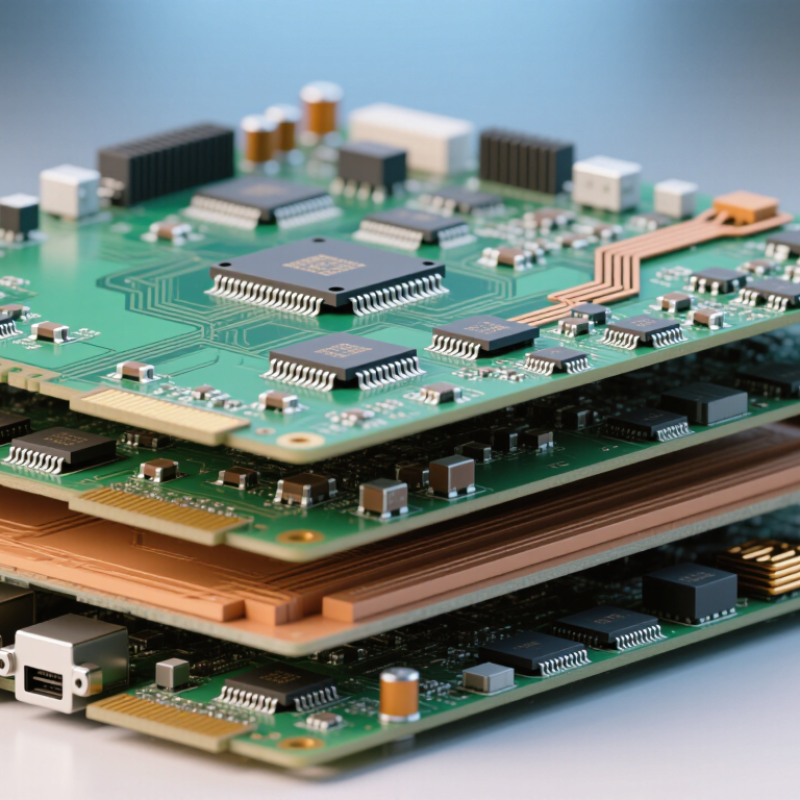
What Is PCB Design and How Does It Work?

What Is PCB Design and How Does It Work?

What is pcb design, and why does it matter in modern electronics? It is the disciplined process of converting a circuit concept into a manufacturable printed circuit board. A designer captures the schematic, selects components, defines footprints, routes traces, and checks electrical and mechanical constraints. The finished board must fit its enclosure, survive manufacturing, and perform reliably in real conditions.

Industry data shows why this work deserves precision. According to the IPC World PCB Production Report, printed circuit boards remain central to automotive, computing, telecommunications, medical, and industrial electronics. Market research from Fortune Business Insights also identifies continued PCB market growth, driven by electric vehicles, connected devices, and advanced computing. These trends increase routing density and shorten development cycles. They also raise the cost of small mistakes.

A practical pcb design workflow often begins with requirements, stack-up planning, and schematic review. Designers then place high-speed interfaces, power components, and heat-producing parts before completing detailed routing. IPC-2221 provides widely used guidance for board design, while IPC-7351 supports land-pattern and component-footprint consistency. A four-layer board may show this clearly: signal layers carry narrow traces, internal planes distribute power and ground, and vias connect the structure through carefully controlled paths.

A schematic can look perfect.

Yet the board may still fail.

Poor return paths, weak thermal relief, incorrect footprints, or insufficient clearance can create expensive rework. That is where simplified explanations become incomplete. Reliable pcb design combines engineering judgment, simulation, design-for-manufacturing reviews, and prototype testing. This guide explains how the process works, where common decisions matter, and why a successful board is designed for both electrons and production reality.

What Is PCB Design and How Does It Work?

PCB Design: Definition, Purpose, and Core Principles

What Is PCB Design and How Does It Work?

PCB Design: Definition, Purpose, and Core Principles

PCB design is the process of planning a printed circuit board that connects electronic components safely and efficiently. Copper traces carry signals and power, while insulating layers prevent unwanted contact. The board acts like a compact road system for electricity. It is not magic.

The purpose is more than making a circuit fit inside a small enclosure. A reliable design must control current, heat, noise, spacing, and mechanical stress. Designers usually begin with a circuit diagram, then arrange components and route traces on the board. Good practice includes short signal paths, clear grounding, suitable trace widths, and enough space around high-voltage areas. Design rules should be checked before fabrication. In practical board reviews, small errors often appear near connectors, mounting holes, and crowded power sections. Experienced designers inspect these areas carefully. Still, even careful work can miss a thermal problem or an unclear label.

Tips: Group related components together. Keep sensitive signals away from noisy power paths. Add test points where measurements may be difficult. Check the board against its circuit diagram, enclosure, and assembly process. Do not trust software warnings alone. A clean report can still hide a poor layout. Use simulation when timing, heat, or signal quality matters. Document every important decision, including choices that later seem imperfect. That record improves review quality and helps future revisions.

Key Components and Layers of a Printed Circuit Board

What Is PCB Design and How Does It Work?

Key Components and Layers of a Printed Circuit Board

A printed circuit board connects electronic components through copper pathways called traces. Its core usually contains a rigid substrate, copper foil, solder mask, and silkscreen. The substrate provides mechanical support. Copper carries electrical signals and power. The solder mask protects exposed copper from oxidation and accidental contact. Silkscreen marks reference numbers, polarity, and test points.

A multilayer PCB adds internal power and ground planes. These layers reduce noise and shorten current paths. A four-layer board often uses signal, ground, power, and signal layers. Vias connect traces between layers. Pads hold components, while through-holes or surface-mount lands support assembly. According to Grand View Research’s 2024 PCB market report, the global market reached approximately 89.7 billion dollars in 2023. The report also projects about 5.6% annual growth through 2030. That growth reflects rising demand for compact, high-density electronics.

Tips: Keep high-speed traces short and reference them to a continuous ground plane. Separate noisy power paths from sensitive analog signals. Follow IPC-2221 design guidance for spacing and current capacity. Check heat flow near regulators and power devices. I have seen layouts pass electrical checks but fail thermal testing. That assumption is convenient, but wrong. Designers should review impedance, drill tolerances, copper thickness, and assembly access together. A small via shift can create a large production problem. Mistakes remain possible, especially when the schematic changes late.

What Is PCB Design and How Does It Work? - Key Components and Layers of a Printed Circuit Board
Category Element Primary Function Typical Materials or Features Design Considerations
Board Structure Substrate Provides mechanical support and electrically separates conductive layers. Commonly a glass-fiber-reinforced epoxy laminate; flexible boards may use polyimide. Material selection affects rigidity, thermal performance, dielectric behavior, and cost.
Board Structure Core Layer Acts as a rigid dielectric layer with copper foil bonded to one or both sides. Pre-cured laminate with a controlled thickness and dielectric constant. Thickness tolerance and layer symmetry influence impedance and board flatness.
Board Structure Prepreg Insulates adjacent copper layers and bonds multilayer sections during lamination. Resin-coated glass fabric that cures under heat and pressure. Resin content and thickness affect spacing, signal impedance, and thermal expansion.
Conductive Layers Copper Traces Carry electrical signals and power between components, vias, and connection points. Patterned copper foil with trace widths defined by current and manufacturing limits. Trace width, spacing, resistance, temperature rise, and signal integrity must be evaluated.
Conductive Layers Power Plane Distributes a relatively stable supply voltage across the circuit. Large copper region connected to a defined power net. Plane shape, return paths, current capacity, and decoupling placement affect performance.
Conductive Layers Ground Plane Provides a low-impedance reference and a return path for current. Continuous or selectively partitioned copper area connected to ground. A continuous reference plane can reduce loop area, noise, and electromagnetic emissions.
Protective Layers Solder Mask Insulates exposed copper and helps prevent solder bridges during assembly. Polymer coating with openings over pads and selected test points. Clearances around pads, coating thickness, and surface cleanliness affect assembly quality.
Protective Layers Silkscreen Displays reference designators, polarity marks, pin indicators, and assembly instructions. Printed ink applied to the component side or solder side. Text should remain readable and should not overlap solderable pads or critical markings.
Connection Features Through-Hole Via Creates an electrical connection through all or most board layers. Plated hole extending through the board thickness. Hole diameter, aspect ratio, annular ring, and layer connections affect reliability.
Connection Features Blind or Buried Via Connects selected outer and inner layers while conserving routing space. Laser-drilled or mechanically drilled plated structure within a multilayer board. Requires controlled fabrication processes and increases manufacturing complexity.
Component Types Resistor Limits current, sets voltage relationships, and provides bias or termination. Passive component specified by resistance value, tolerance, and power rating. Power dissipation, tolerance, placement, and thermal spacing must match the circuit requirement.
Component Types Capacitor Stores electrical charge, filters noise, couples signals, or stabilizes supply voltage. Passive component specified by capacitance, voltage rating, and dielectric type. High-frequency decoupling capacitors should be placed close to the relevant power pins.
Component Types Inductor Stores energy in a magnetic field and supports filtering, energy conversion, or impedance matching. Coil or multilayer magnetic component with a specified inductance and current rating. Inductance tolerance, saturation current, magnetic coupling, and heat must be considered.
Component Types Diode Controls current direction, protects against voltage transients, or converts alternating current. Semiconductor device with forward-voltage and reverse-voltage specifications. Peak current, reverse recovery, thermal dissipation, and orientation are important.
Component Types Integrated Circuit Performs processing, control, amplification, conversion, memory, or interface functions. Packaged semiconductor with multiple electrical pins and a defined footprint. Pin escape routing, power integrity, thermal management, and signal integrity are key concerns.
Component Types Connector Provides a removable electrical or mechanical interface to another board, cable, or system. Through-hole or surface-mount part with contacts, housing, and mechanical retention features. Mechanical load, pin arrangement, current rating, mating cycles, and access clearance matter.
Mounting Methods Surface-Mount Technology Mounts components directly onto pads on the board surface. Compact components with solder pads on one or both sides of the PCB. Supports high component density but requires accurate land patterns and controlled assembly.
Mounting Methods Through-Hole Technology Mounts components using leads inserted through drilled holes. Leaded components soldered on the opposite side or in plated holes. Provides strong mechanical attachment but generally requires more board area.
Layer Configurations Single-Layer PCB Routes conductors on one copper layer with components generally placed on one side. One conductive layer over a dielectric substrate. Suitable for simple, low-density circuits; routing space and return paths are limited.
Layer Configurations Double-Layer PCB Uses copper on both sides to provide more routing area and component flexibility. Two conductive layers separated by an insulating substrate. Vias connect the two sides; careful grounding and routing reduce interference.
Layer Configurations Multilayer PCB Combines multiple signal, power, and ground layers in a laminated structure. Alternating copper and dielectric layers bonded under heat and pressure. Enables high density and controlled impedance but requires precise stack-up planning.
Design Workflow Schematic Capture Defines the logical electrical relationships among components and nets. Symbols, net names, power connections, and design rules represented in electronic design software. Correct connectivity and component attributes are essential before physical layout begins.
Design Workflow PCB Layout Transforms the schematic into physical footprints, routes, planes, and board geometry. Component placement, copper tracks, vias, keep-outs, mounting holes, and layer stack-up. Designers balance electrical performance, manufacturability, thermal behavior, and mechanical fit.
Design Verification Design Rule Check Identifies violations of spacing, connectivity, clearance, and manufacturing constraints. Automated checks based on configured electrical and fabrication rules. Rules should reflect the selected manufacturing process rather than generic defaults alone.
Design Verification Signal Integrity Analysis Evaluates waveform quality, timing, reflections, crosstalk, and transmission-line effects. Simulation or calculation using trace geometry, dielectric properties, and driver characteristics. Controlled impedance, short return paths, termination, and layer transitions can improve results.
Design Verification Thermal Analysis Estimates temperature rise and identifies heat concentration in components or copper areas. Power dissipation, copper spreading, thermal vias, airflow, and enclosure conditions. Components with higher power dissipation need adequate copper area and clearance.
Manufacturing Fabrication Data Communicates board geometry, drill information, layer data, and manufacturing notes. Standardized manufacturing files, drill files, stack-up details, and fabrication drawings. Data should be reviewed for layer order, hole types, dimensions, tolerances, and revisions.
Manufacturing Assembly and Testing Places and solders components, then verifies electrical and functional performance. Automated or manual assembly followed by visual inspection, electrical tests, and functional tests. Test points, component accessibility, polarity markings, and inspection standards should be planned early.

The Step-by-Step Process of Creating a PCB

What Is PCB Design and How Does It Work?

PCB design turns an electrical idea into a physical circuit board. The process begins with clear requirements, such as power limits, board size, signal speed, and operating conditions. Engineers then draw a schematic showing how each component connects. Component availability matters here. A perfect part on paper may be difficult to source or unsuitable for production.

The schematic becomes a board layout. Designers place connectors and major components first, keeping signal paths short and practical. They route copper traces, add power and ground structures, and check spacing between conductive areas. Heat-producing parts may need extra copper for cooling. Design-rule checks can detect narrow traces, unwanted connections, or insufficient clearance. These tools help, but they do not replace careful review. A small oversight can still survive.

Tips: Keep high-speed traces short. Separate noisy power sections from sensitive signals. Add clear reference labels. Review the board from a manufacturing perspective, not only an electrical one. Prototype files usually include fabrication drawings, drill data, and assembly details. After the first board arrives, engineers inspect solder joints, measure key voltages, and test the circuit under realistic loads. Problems often appear during this stage. A connector may be awkward to reach, or a trace may run too close to a heat source. That feedback leads to layout changes, and sometimes the second version is much better.

How PCB Layouts Become Manufactured Circuit Boards

PCB design turns electrical intent into copper, laminate, holes, and inspected assemblies. The work begins with a schematic showing how components should connect. Engineers then assign footprints, define board layers, and route traces between pads. Power paths need wider copper. High-speed signals need controlled spacing and impedance.

The layout becomes physical through a disciplined manufacturing flow. Gerber or ODB++ files describe copper patterns, drill locations, solder masks, and legends. A fabricator images each layer onto copper-coated material. Etching removes unwanted copper, while pressing bonds the layers together. Drilling creates vias and component holes. Plating strengthens those holes and connects internal copper layers. After solder-mask coating, surface finishing, electrical testing, and inspection, the bare board reaches assembly.

Small errors matter.

A misplaced decimal can change a trace width. A missing courtyard can block a connector. IPC-2221 and IPC-A-600 provide widely used design and acceptance guidance for these decisions. Grand View Research’s 2024 Printed Circuit Board Market report estimated the global market at about 89.7 billion dollars in 2023, with a projected 5.6% compound annual growth rate through 2030. That growth increases pressure on reliable design-for-manufacturing practices. In real reviews, the first layout is rarely perfect. A clean screen can still hide an untested assumption. Teams should check fabrication limits early, not after releasing files.

Testing, Debugging, and Improving PCB Designs

What Is PCB Design and How Does It Work?

Testing starts before power reaches the board. A design review should inspect traces, clearances, grounding, thermal paths, and component footprints. In practice, a clean schematic can still produce a failed prototype. I have seen one reversed connector footprint waste days of testing. Measure twice. Power up slowly. Record every voltage, temperature, and unexpected sound.

Debugging works best when symptoms become evidence. Use a current-limited supply, oscilloscope, multimeter, and thermal camera. Check the power rail first, then clocks, signals, and interfaces. NIST’s 2022 report estimated that poor software quality costs the United States about $2.41 trillion annually. PCB defects are different, but the lesson remains relevant: late corrections are expensive. IPC industry outlook reports also continue to identify material costs and skilled-labor shortages as major manufacturing pressures. Early validation protects both time and yield.

Tips: Test one change at a time. Compare measured values with simulations. Mark every tested node on a printed layout. Keep failed boards; they reveal patterns. Automated optical inspection can catch solder and placement defects, but it cannot replace functional testing. Environmental checks may expose failures caused by heat, vibration, or humidity. Improvement should follow evidence, not instinct. Still, models can be wrong. Recheck assumptions when the board behaves unexpectedly.

PCB Design Reference: Copper Weight vs. Nominal Thickness

Copper thickness is a practical PCB design parameter used when checking fabrication results, current-carrying capability, thermal performance, and design-rule assumptions. One ounce of copper is approximately 35 micrometers thick.

During testing and debugging, comparing the manufactured copper thickness with the nominal design value can help identify unexpected voltage drop, heating, or trace-performance issues.